Site pages
Current course
Participants
General
MODULE 1.
MODULE 2.
MODULE 3.
MODULE 4.
MODULE 5.
MODULE 6.
MODULE 7.
MODULE 8.
MODULE 9.
MODULE 10.
MODULE 11.
MODULE 12.
MODULE 13.
MODULE 14.
MODULE 15.
MODULE 16.
MODULE 17.
MODULE 18.
MODULE 19.
Lecture 6 Active positive limiter, Active positive clamper,Active peak detector clipper and clamper circuit
Active positive limiter
Figure 6.1 shows an active positive limiter circuit, which clips off a part of the signal. The input and output signals are also shown. When the moving contact of the resistor Vref is positive, the error voltage causes a negative output voltage and the diode is turned on. Since the feedback resistance is zero, a heavy negative feedback is produced. The output is zero for all positive values of vi. When vi is negative, the output of op amp, is positive and the diode is truned off. Thus, the feedback loop is opened and the output va follows the negative half of the input vi. Thus, the positive half is dipped off. To change the clipping level, we can adjust V ref. Then the clipping occurs at Vref.
Active positive clamper
Figure 6.2 shows a positive clamper circuit using op amp. This circuits adds a de component to the input signal. The input and output signals are also shown.
During the first negative half cycle of the input signal, we get a positive output and the diode is turned on. Due to the presence of the virtual ground, the capacitor C is charged to peak value Vm of the input signal with the polarity as shown. As the input signal turns positive, the diode is turned off (because the output is now negative). The virtual ground is lost. The output voltage is the sum of the signal and Vm.
Active peak detector
Figure 6.3 shows an op amp circuit for peak detection of low lwvel signals. The closed loop knee voltage is very small (in the mirco volt region). When the diode is on, the heavy voltage feedback producers an output impedance which is nearly zero. Thus, the charging time of the capacitor C is very small and the capacitor charges quickly to the positive peak value. When the diode is off, the capacitor tends to discharge through load resistor RL. It time constant RL C is much longer as compared to the period of the input signal, we can achieve peak detection of low level signals.
Comparator
A comparator is the simplest circuit that moves signals between the analog and digital worlds.
What does a comparator do?
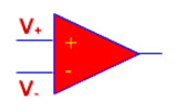
Simply put, a comparator compares two analog signals and produces a one bit digital signal. The symbol for a comparator is shown below.
The comparator output satisfies the following rules:
-
When V+ is larger than V- the output bit is 1.
-
When V+ is smaller than V- the output bit is 0
When an op amp is used in open loop configuration, an input signal, as small as 1 m V (or even lower) van saturates the op amp. Therefore, the output will be between the maximum and minimum limits imposed by the dc supply. This action is unsuitable for linear circuits. However, in digital circuits only the highest and lowest voltages are the meaningful values as they can be used to represent the binary numbers 0 and 1.
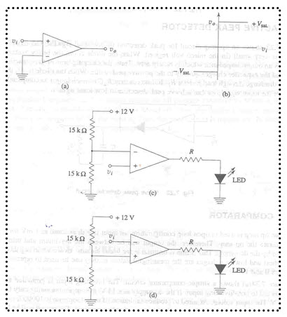
Figure 6.4 (a) shows a simple comparator circuit. The inverting input is grounded and the input signal is fed to non-inverting input. If the dc supply is +/- 15 V, the output can swing only from –13.5 to +13.5V. The input voltage required to produce saturation (if open loop gain is 100000) is 13.5 /100000 or 0.135 mV. Let an input of 1V be applied to non-inverting terminal. The output will be limited to the maximum value of + 13.5 V. If the input signal is reduced, the output will remain at +13.5V. Only when the input is less than 0.135 mV will the output fall. For any input higher than 0.135 mV, the output will be 13.5 V. If the signal is negative, a similar action will occur. Any input signal more negative than –0.135 m V will produce an output o f-13.5V. Since 0.135mVis a very small value, the graph of output voltage will show a vertical transistor from –V to V as the input signal goes from negative to positive as shown in Fig. 6.4(b).
It is also possible to operate the circuit of Fig.6.4 (a) with non-inverting terminal grounded and the signal applied to inverting terminal. Now a positive input (more than 0.135 mV) will cause negative output saturation delivering an output of –13.5 V. Similarly, an input more negative than –0.135 mV will cause an output of +13.5V.
The Circuit of Fig 6.4 (a) does also know as zero crossing detectors.
In Fig. 6.4(a), the reference level has been set at zero (by grounding the inverting terminal). In general the reference level need not be zero but can be any; desired positive or negative voltage. Moreover, the reference voltage can be connected to either the inverting terminal or non-inverting terminal and the input applied to the other terminal.
Figure 6.4(c) shows the reference voltage applied to minus input, (i.e., inverting input) and output connected to an LED. The reference voltage level is,
Since the reference level is connected to inverting, i.e., terminal, the output vo will got to positive saturation level whenever the input v is more than +6V and LED will become on, thus, indicating that input is less positive than reference level.
Figure 6.4(d) shows the reference voltage connected to non-inverting (or +) terminal. Any input v less than reference level of +6V will cause the output to switch on the LED, indicating that input is less than reference level.The comparator has many applications in signal processing and wave shaping circuits. In each such application, the comparator detects whether the applied signal is more or less than the reference level.
Clampers:
A clamper is an electronic circuit that prevents a signal from exceeding a certain defined magnitude by shifting its DC value. The clamper does not restrict the peak-to-peak excursion of the signal, but moves it up or down by a fixed value. A diode clamp (a simple, common type) relies on a diode, which conducts electric current in only one direction; resistors and capacitors in the circuit are used to maintain an altered dc level at the clamper output.
General function:
A clamping circuit (also known as a clamper) will bind the upper or lower extreme of a waveform to a fixed DC voltage level. These circuits are also known as DC voltage restorers. Clampers can be constructed in both positive and negative polarities. When unbiased, clamping circuits will fix the voltage lower limit (or upper limit, in the case of negative clampers) to 0 Volts. These circuits clamp a peak of a waveform to a specific DC level compared with a capacitively coupled signal which swings about its average DC level
Types:
Clamp circuits are categorized by their operation; negative or positive and biased and unbiased. A positive clamp circuit outputs a purely positive waveform from an input signal; it offsets the input signal so that all of the waveform is greater than 0 V. A negative clamp is the opposite of this - this clamp outputs a purely negative waveform from an input signal.A bias voltage between the diode and ground offsets the output voltage by that amount.For example, an input signal of peak value 5 V (VIN = 5 V) is applied to a positive clamp with a bias of 3 V (VBIAS = 3 V), the peak output voltage will be
VOUT = 2VIN + VBIAS
VOUT = 2 * 5 V + 3 V
VOUT = 13 V
Positive unbiased:

In the negative cycle of the input AC signal, the diode is forward biased and conducts, charging the capacitor to the peak positive value of VIN. During the positive cycle, the diode is reverse biased and thus does not conduct. The output voltage is therefore equal to the voltage stored in the capacitor plus the input voltage gain, so VOUT = 2VIN
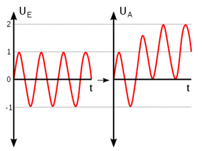
Positive unbiased voltage clamping shifts the amplitude of the input waveform so that all parts of it are greater than 0 V
Negative unbiased:
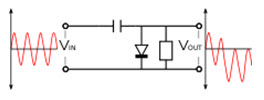
A negative unbiased clamp is the opposite of the equivalent positive clamp. In the positive cycle of the input AC signal, the diode is forward biased and conducts, charging the capacitor to the peak value of VIN. During the negative cycle, the diode is reverse biased and thus does not conduct. The output voltage is therefore equal to the voltage stored in the capacitor plus the input voltage again, so
VOUT = -2VIN
Positive biased:
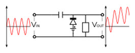
A positive biased voltage clamp is identical to an equivalent unbiased clamp but with the output voltage offset by the bias amount VBIAS. Thus,
VOUT = 2VIN + VBIAS
Negative biased:
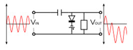 A negative biased voltage clamp is likewise identical to an equivalent unbiased clamp but with the output voltage offset in the negative direction by the bias amount VBIAS. Thus,
VOUT = -2VIN - VBIAS