Site pages
Current course
Participants
General
MODULE 1.
MODULE 2.
MODULE 3.
MODULE 4.
MODULE 5.
MODULE 6.
MODULE 7.
MODULE 8.
MODULE 9.
MODULE 10.
LESSON 2. Semiconductor-P& N type-drift and diffusion current- PN junction as diode.
SEMICONDUCTORS
A semiconductor is a substance which has receptivity in between conductors and insulators (e.g) germanium, silicon carbon etc.
Bonds in Semiconductor
The atoms of every element are held together by the bonding action of valence electrons. This makes the atom more active to enter into bargain with the other atom to acquire eight electrons in the last orbit. During this process the atom may lose, gain or share valence electrons with other atoms. In this case, there is only sharing of one or more valence electrons between the two atoms, each of which tries to fill up its outer most orbit. Such bonds are called covalent bonds. The germanium atom has four valence electrons in the outer most orbit. As seen each germanium atom shares one electron each with four surrounding atoms. In this way the central atom setup covalent bonds.
At 0OK, all electrons in the covalent bonds are firmly held, there is no free carriers and hence becomes an insulator. However at room temperature some of the covalent bonds will be broken, because of the thermal energy applied to the crystal. In this way be the movement of free electron, holes are filled up and created.
The electron in the valence band moves away leaving a hole in its place. It is relatively easy for a valence electron in a neighboring atom to leave its covalent bond to fill this hole. An electron moving from a band to fill a hole leaves in its initial position. Hence the hole effectively moves in the direction opposite to electron and so electron-hole pairs are generated, when temperature of semiconductor is increased.
For each created electron-hole pair, two charge carrying particles are formed. One is free electron and the other is the hole. These particles move in opposite direction in an electric field, but since they are opposite sign, the current of each is in the same direction.
Conductivity of Pure Germanium
Fig. (2.1) shows the motion of free electrons and holes in a pure germanium when an external electrical field is applied.
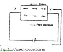
When the direction of the electrical field is from right to left as shown in Fig 2.1, the free electrons are pulled towards the right side whereas the holes are pulled towards the left side. The pulling forces are superimposed upon the thermal random motion of the free electrons and poles. The free electrons move from (point M) left to right and reaches point V, after some time. The net distance travelled. During the travel it collides with atoms at points N,O,P,Q,R,S,T and U. The net displacement of the electron is the cause for the flow of electric current. The conventional direction of electric current is just opposite to the flow of electrons.
In the same manner the holes are pulled towards the left side (negative electrodes). Assume that a hole is existing at point I Due to thermal energy the covalent band breaks. The electron escapes from the structure and thus a hole is formed. This is only for short time duration. Due to thermal agitation the electron kept at G may move to position I and thus once again the bond is completed. In turn a hole is created at junction G. In such a way hole is created at F,E,D, B and A. Thus the hole is displaced from I to A. This kind of displacement is called hole motion which is also the cause for the electric current.
Therefore, there exists two kind of charge namely electrons and holes in a pure germanium. The conductivity of pure germanium depends upon the mobile charge carriers and also their mobility.
Types of Semiconductor
Semiconductor may be classified as follows:
- Intrinsic or pure semiconductor
- Extrinsic or impure semiconductor
Intrinsic Semiconductor
Pure semiconductor is known as an intrinsic semi-conductor. Pure germanium and silicon are common examples. These semiconductors have four valence electrons which are easily affected by external influences. Covalent bond is formed only by means of these electrons with the neighboring atoms.
The last orbit electrons (valence electrons) energy are shared with neighboring atoms and hence each atom is surrounded by a completely filled orbits at 0°K. These materials behave as perfect insulator. But even at room temperature hole-electron pairs are produced. When external electric field is applied across the intrinsic semiconductor the current conduction take place. That current conduction is due to free electrons and holes. The number of electrons is equal to the number of holes in an intrinsic semiconductor at room temperature. The energy gap is moderate of an intrinsic semiconductor (pure. germanium) At 0°K the valence band is completely filled with electrons and the conduction, band is empty, Fermi level is nothing but the energy which corresponds to the centre of gravity of conduction electrons and holes.
Extrinsic Semiconductors
A pure semiconductor is called intrinsic semiconductor. The only current carriers in this pure semiconductor are electron hole pairs. In most of the applications, these produce feeble current. So, for increasing either the number of free electrons or the number of holes, some impurity atoms are added with the pure semiconductor. This adding process is called doping. After the impurity atoms are doped with pure semiconductor it is called an extrinsic Semiconductor.
Depending upon the types of impurity atoms that have been added with the pure semiconductor, the extrinsic semiconductor is classified as
a) P-type semiconductor
b) N-type semiconductor
P-type Semiconductor
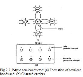 Let us consider a germanium crystal. The germanium atom has four valence electrons. If we doped with an impurity atom of having only three electrons (Boron atom) in its valence band with this germanium atom, a new crystal is formed. The new crystal will have its structure and energy band diagram as shown in Fig.2.2. In this newly formed extrinsic semiconductor we find that a trivalent atom is in between four neighboring germanium atoms as shown in Fig. 2.2. It is further noted that only seven electrons travel in its valence orbits. In other words one hole appears in each trivalent atom. The number of holes in the doped crystal can be increased by adding more number of impurity atoms.
A pure semiconductor doped by trivalent (aluminium, boron and gallium) impurity is known as P-type semiconductor . In this P-type semiconductor, conduction is by means of holes in the valence band. So the holes are considered as majority carries in P-type semi-conductor whereas electrons are minority carriers. The trivalent provide room for the germanium atom. If the trivalent impurity is added with germanium the new extrinsic crystal is formed as shown in Fig. 1.3. The strong force holding the structure is called convalent bond. The minimum heat energy required to break the germanium extrinsic covalent bond is 0.1 eV and 0.05ev for silicon extrinsic semiconductor. In this type, concentration of electrons is in the conduction band. Conduction is by the hole movement in the valence band. The acceptor level accopts the electrons from the valence band.
N-type Semiconductor
If pentavalent impurities are added with extrinsic semiconductor a new crystal is formed. 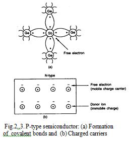 The new crystal will have its structure and energy band diagram as shown in Fig 2.3. In this structure, we find that a pentavalent atom is in between four neighboring germanium atoms. After forming covalent bonds with four neighbors, this central atom has an extra electron left over. Since the valence orbit cannot hold more than eight electrons, the extra electron must travel in a conduction band orbit. Since each pentavalent atom denote one electron, the number of electrons in this structure can be increased by doping of more number of impurity atoms. Suitable pentavalent impurities are antimony, and arsenic.
In N-type extrinsic semiconductor adding of pentavalent impurity like antimony (Sb) increases the number of conduction electrons. Hence, concentration of electrons in the conduction band is increased and exceeds the concentration of holes in the valence band. Due to this 'Fermi level shifts upwards towards the bottom of the conduction band .The energy level for fifth electron (donor level) is 0.001eV below the conduction band for germanium and 0.05eV for silicon. In this type of extrinsic semiconductor, conduction is by means of electrons which are called the majority carriers whereas holes are called minority carriers.
Drift current
A pure semiconductor at 0º Kevin behave as an insulator. When the temperature is raised above absolute zero more electrons are detached from the covalent bond. Thus the electron-hole pairs are increased, when the temperature is raised. These free electrons and holes move in random manner. When the electric field is applied across the semiconductor bar, it forces the randomly moving electron-hole pairs in its direction (field direction). This causes a current flow in the circuit. This current is called drift current.
Diffusion current
Let us assume that one type of charge carriers concentration is accumulated at one end of piece of semiconductor material. Since the charge carries are all the same polarity there is a force of repulsion between them. The result is that there is a tendency for the charge density to one of low density. This movement continues until all the carriers are evenly distributed throughout the material. Thus the movement of charge carriers constitutes an electric current. This type of current is known as diffusion current.
P-N Junction as diode
The simplest semiconductor device has to region, one regions doped with p-type impurity and the second region doped the n type impurity. The impurity concentrate changes from donar to acceptor at boundary.
a. Depletion region
Both the region have equal positive and negative charges and are electrically neutral. However the n-type has more free electron then holes and p-type has more holes and p-type has more holes than free electron. The free electron on n-type material tend to diffuse. Each electron diffuse across the juctia into the p-type one. Each electron diffusia from the n-region into the p-region leaves a positive charges behind in the n-region. Similarly the holes in the p-type material diffuse across the junction into the n-region leavings negatives charges behind. As this the n-region leavings negatives charges behind. As this diffusion occurs, then-region becomes positively charged and the p-region becomes negatively charged. Due to this displacement of charges, an electric field appears at the junction. Equilibrium is established when this field large enough to restrain further diffusion. The holes which neutralized the acceptor ion hear the junction in the p-type materials disappear due to recombinant with electron which have diffused from n-type materials across the junction. Later wise, the neutralizing electron in the n-type material combine with the holes which have crossed the junction from the p-type material. The electron charges are confined to the neighbourhood of the junction and consists of in mobile ions. Since the region around the function in depleted of mobile charges it is known a depletion region or transit region or the space charge region. The width of this depletion region is about 10-4 cm. There is an equilibrium potential difference vs across the depletion region.
b. Barrier potential
The equilibrium potential across the depletion region is known a barrier potential. At 25°C the barrier potential. At 25°C the barrier potential is 0.3 V for germanium and 0.74 for silica diode. The temperature at the junction of p and n-type materials is known as function temperature and more to different than the ambient temperature. The barrier potential depend as the junction temperature. At higher junction temperature more hole and free electron present. This mean a reduction in the width of the depletion layer, this decreasing the barrier potential. For each ie. Rise 1a junction temperature, the barrier potential of both silicon and germicum decreased by 2 mV.
When a diode is forward biased, the current remain zero till applied voltage overcomes the barrier potential. Therefore in a silicon diode biased in forward direction, the current flows in the circuit only when the applied voltage is more than 0.7 V.
c. Effect of forward bias
The forward bias is applied by connecting the terminal of a battery to p-type material and the negative battery terminal to n-type material. The potential and the P-type material is raised (art to n-type material) and an electric field is set up. The terminal of the battery removes electron from p material leaving holes there. The negative terminal of the battery inject electron into n material. As a result of the above, the width of the depletion bore is reduced. The free electron cross the junction from n-type to p-type and holes from p-type to n-type. These majority carriers travel around the closed loop and a steady current flows in the circuit through p-n junction. This connection is also known as the easy current direction.
Effect of reverse bias
The p-n junction is reverse biased when the terminal of the battery is connected to the n-type material and –ve terminal to P–type material. The polants the connector cause be holes in P–type and electron in P–type materials to move away from the junction. Here by increasing the depletion region. The current in normally zero.
Thus the P – type junction ha prospects of conducting current only when biased in the forward direct and water as a diode.
Effect of short circuit
When a P- type junction in short circuited no current can flow in the circuit, the electrostatic potential remain of the fans value as that rather open circuit condition.
Last modified: Wednesday, 4 December 2013, 10:39 AM