Site pages
Current course
Participants
General
MODULE 1.
MODULE 2.
MODULE 3.
MODULE 4.
MODULE 5.
MODULE 6.
MODULE 7.
MODULE 8.
MODULE 9.
MODULE 10.
LESSON 5. Full wave rectifier with RC filter- Zener diode circuit- multiple diode circuits-photo diode and LED circuit.
Filters, Ripple Voltage, and Diode Current
If a capacitor is added in parallel with the load resistor of a half-wave rectifier to form a simple filter circuit (Figure 5.1(a)), we can begin to transform the half-wave sinusoidal output into a dc voltage. Figure 5.2(b) shows the positive half of the output sine wave, and the beginning portion of the voltage across the capacitor, assuming the capacitor is initially uncharged.
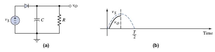
When the signal voltage reaches its peak and begins to decrease, the voltage across the capacitor also starts to decrease, which means the capacitor starts to discharge. The only discharge current path is through the resistor. If the RC time constant is large, the voltage across the capacitor discharges exponentially with time (Figure 2.8(c)). During this time period, the diode is cut-off.
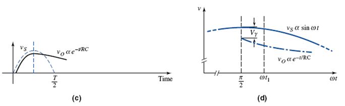
A more detailed analysis of the circuit response when the input voltage is near its peak value indicates a subtle difference between actual circuit operation and the qualitative description. If we assume that the diode turns off immediately when the input voltage starts to decrease from its peak value, then the output voltage will decrease exponentially with time, as previously indicated. An exaggerated sketch of these two voltages is shown in Figure 5.1(d). The output voltage decreases at a faster rate than the input voltage,which means that at time t1 the voltage across the diode, is greater than Vγ. However, this condition cannot exist and the diode does not turn off immediately. If the RC time constant is large, there is only a small difference between the time of the peak input voltage and the time the diode turns off.
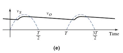
During the next positive cycle of the input voltage, there is a point at which the input voltage is greater than the capacitor voltage, and the diode turns back on. The diode remains on until the input reaches its peak value and the capacitor voltage is completely recharged.
Since the capacitor filters out a large portion of the sinusoidal signal, it is called a filter capacitor. The steady-state output voltage of the RC filter is shown in Figure 5.1 e).
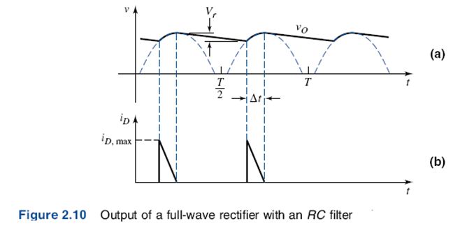
The ripple effect in the output from a full-wave filtered rectifier circuit can be seen in the output waveform in Figure 5.2.
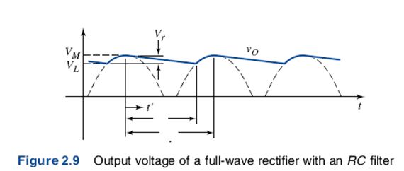
The capacitor charges to its peak voltage value when the input signal is at its peak value. As the input decreases, the diode becomes reverse biased and the capacitor discharges through the output resistance R. Determining the ripple voltage is necessary for the design of a circuit with an acceptable amount of ripple.
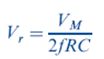
If we can assume that the ripple effect is small we get the following approximation
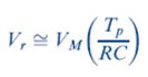
where Tp is the time between peak values of the output voltage.
For a full-wave rectifier Tp is one-half the signal period. Therefore, we can relate Tp to the signal frequency,

and the ripple voltage becomes
The diode in a filtered rectifier circuit conducts for a brief interval Δt near the peak of the sinusoidal input signal (Figure 5.3a).
ZENER DIODE CIRCUITS
The breakdown voltage of a Zener diode was nearly constant over a wide range of reverse-bias currents. This makes the Zener diode useful as a voltage regulator, or a constant-voltage reference circuit. In this chapter, we will look at an ideal voltage reference circuit, and the effects of including a non-ideal Zener resistance.
The results of this section will then complete the design of the electronic power supply .We should note that in actual power supply designs, the voltage regulator will be a more sophisticated integrated circuit rather than the simpler Zener diode design that will be developed here. One reason is that a standard Zener diode with a particular desired breakdown voltage may not be available.
Ideal Voltage Reference Circuit
Figure 5.4 shows a Zener voltage regulator circuit. For this circuit, the output voltage should remain constant, even when the output load resistance varies over a fairly wide range, and when the input voltage varies over a specific range.
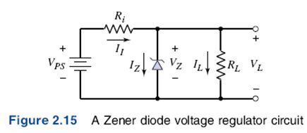
We first determine the proper input resistance Ri. This resistance limits the current through the Zener diode and drops the excess voltage between VPS and VZ.
![]()
which assumes that the Zener resistance is zero for the ideal diode. Solving this equation for the diode current. Iz, we get
![]()
where 1L = Vz / RL, and the variables are the input voltage source VPS and the load current 1L.
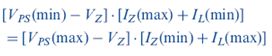
For proper operation of this circuit, the diode must remain in the breakdown region and the power dissipation in the diode must not exceed its rated value. In other words:
- The current in the diode is a minimum, Iz(rnin), when the load current is a maximum, IL(max), and the source voltage is a minimum, VPS(min).
- The current in the diode is a maximum, Iz(max), when the load current is a minimum, IL(min), and the source voltage is a maximum, VPS(max).
Inserting these two specifications into the previous equation, we obtain
![]()
and
![]()
Equating these two expressions, we then obtain
Reasonably, we can assume that we know the range of input voltage, the range of output load current, and the Zener voltage. The previous equation then contains two unknowns Iz(min) and Iz(max). Further, as a minimum requirement, we can set the minimum Zener current to be one-tenth the maximum Zener current, or IZ(min) =0.1 IZ(max). We can then solve for IZ(max), using the previous equation, as follows:
![]()
Use the maximum current obtained from the above equation, we can determine the maximum required power rating of the Zener diode. Then we can determine the required value of the input resistance using one of the previous equations.
MULTIPLE-DIODE CIRCUITS
Since a diode is a nonlinear device, part of the analysis of a diode circuit involves determining whether the diode is "on" or "off." If a circuit contains more than one diode, the analysis is complicated by the various possible combinations of "on" and "off.”
In this section, we will look at several multiple-diode circuits. We will see, for example, how diode circuits can be used to perform logic functions.
Example Diode Circuits
To review briefly, consider two single-diode circuits. Figure 5.5(a) shows a diode in series with a resistor. A plot of voltage transfer characteristics, v0 versus vI , shows the piecewise linear nature of this circuit (Figure 5.5{b)).
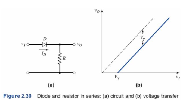 The diode does not begin to conduct until vI = Vγ . Consequently, for vI < Vγ the output voltage is zero; for vI > Vγ the output voltage is vo = vI - Vγ .
Figure 5.6(a) shows a similar diode circuit, but with the input voltage source explicitly included to show that there is a path for the diode current. The voltage transfer characteristic is shown in Figure 5.6(b).
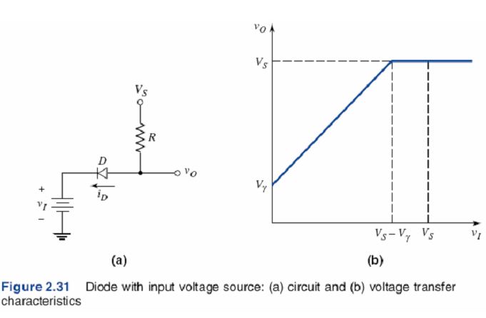
In this circuit, the diode remains conducting for vI < VS - Vγ , and the output voltage is v0 = vI + Vγ . When vI > VS - Vγ , the diode turns off and the current through the resistor is zero; therefore, the output remains constant at VS.
In multidiode circuits, each diode may be either "on" or "off." Consider the two-diode circuit in Figure 5.7. Since each diode may be either on or off, the circuit has four possible states. However, some of these states may not be feasible because of diode directions and voltage polarities.
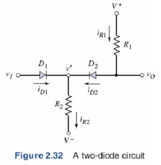
If we assume that V+ > V- and that V+ - V- > Vγ , there is a possibility that D2 can be turned on. Figure 5.8 shows the resulting plot of vo versus vI .
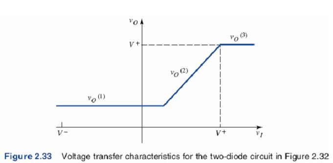
Three distinct regions are shown, corresponding to the various conducting states of Dl and D2. The fourth possible state, corresponding to both diodes being off, is not feasible in this circuit
PHOTODIODE AND LED CIRCUITS
A photodiode converts an optical signal into an electrical current and a light-emitting diode (LED) transforms an electrical current into an optical signal.
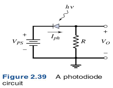
Photodiode Circuit
Figure 5.9 shows a typical photodiode circuit in which a reverse-bias voltage is applied to the photodiode. If the photon intensity is zero, the only current through the diode is the reverse-saturation current, which is normally very small. Photons striking the diode create excess electrons and holes in the space-charge region, where the electric field quickly separates these excess carriers and sweeps them out of the space-charge region, creating a photocurrent in the reverse-bias direction.
LED Circuit
A light-emitting diode (LED) is the inverse of a photodiode; that is, a current is converted into an optical signal. If the diode is forward biased, electrons and holes are injected across the space-charge region, where they become excess minority carriers. These excess minority carriers diffuse into the neutral n and p regions, where they recombine with majority carriers, and the recombination can result in the emission of a photo (with a direct band gap material such as GaAs).
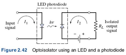
One application of LEDs and photodiodes is in opto-isolators, in which the input signal is electrically decoupled from the output (Figure 5.10). An input signal applied to the LED generates light, which is subsequently detected by the photodiode. The photodiode then converts the light back to an electrical signal. There is no electrical feedback or interaction between the output and input portions of the circuit.
Last modified: Wednesday, 4 December 2013, 10:44 AM