Site pages
Current course
Participants
General
MODULE 1.
MODULE 2.
MODULE 3.
MODULE 4.
MODULE 5.
MODULE 6.
MODULE 7.
MODULE 8.
MODULE 9.
MODULE 10.
LESSON 9. NPN transistor configurations- α and β relationship- Input and output characteristics-PNP transistor-configurations and circuits
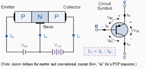
The NPN Transistor
Bipolar Transistor or BJT, comes in two basic forms. An NPN (Negative-Positive-Negative) type and a PNP (Positive-Negative-Positive) type, with the most commonly used transistor type being the NPN Transistor. We also learnt that the transistor junctions can be biased in one of three different ways - Common Base, Common Emitter and Common Collector. In this tutorial we will look more closely at the "Common Emitter" configuration using NPN Transistors with an example of the construction of a NPN transistor along with the transistors current flow characteristics is given below.
An NPN Transistor Configuration
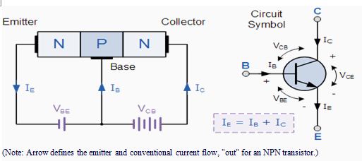
The construction and terminal voltages for an NPN transistor are shown above. The voltage between the Base and Emitter ( VBE ), is positive at the Base and negative at the Emitter because for an NPN transistor, the Base terminal is always positive with respect to the Emitter. Also the Collector supply voltage is positive with respect to the Emitter ( VCE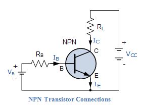 ). So for an NPN transistor to conduct the Collector is always more positive with respect to both the Base and the Emitter. Then the voltage sources are connected to an NPN transistor as shown. The Collector is connected to the supply voltage VCC via the load resistor, RL which also acts to limit the maximum current flowing through the device. The Base supply voltage VB is connected to the Base resistor RB, which again is used to limit the maximum Base current.
We know that the transistor is a "current" operated device (Beta model) and that a large current ( Ic ) flows freely through the device between the collector and the emitter terminals when the transistor is switched "fully-ON". However, this only happens when a small biasing current ( Ib ) is flowing into the base terminal of the transistor at the same time thus allowing the Base to act as a sort of current control input.
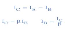
The transistor current in an NPN transistor is the ratio of these two currents ( Ic/Ib ), called the DC Current Gain of the device and is given the symbol of hfe or nowadays Beta, ( β ). The value of β can be large up to 200 for standard transistors, and it is this large ratio between Ic and Ib that makes the NPN transistor a useful amplifying device when used in its active region as Ib provides the input and Ic provides the output. Note that Beta has no units as it is a ratio.
Also, the current gain of the transistor from the Collector terminal to the Emitter terminal, Ic/Ie, is called Alpha, ( α ), and is a function of the transistor itself (electrons diffusing across the junction). As the emitter current Ie is the product of a very small base current plus a very large collector current, the value of alpha α, is very close to unity, and for a typical low-power signal transistor this value ranges from about 0.950 to 0.999
α and β Relationship in a NPN Transistor
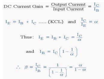
By combining the two parameters α and β we can produce two mathematical expressions that gives the relationship between the different currents flowing in the transistor.
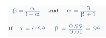
The values of Beta vary from about 20 for high current power transistors to well over 1000 for high frequency low power type bipolar transistors. The value of Beta for most standard NPN transistors can be found in the manufactures datasheets but generally range between 50 - 200.
The equation above for Beta can also be re-arranged to make Ic as the subject, and with a zero base current ( Ib = 0 ) the resultant collector current Ic will also be zero, ( β x 0 ). Also when the base current is high the corresponding collector current will also be high resulting in the base current controlling the collector current. One of the most important properties of the Bipolar Junction Transistor is that a small base current can control a much larger collector current. Consider the following example.
The Common Emitter Configuration.
As well as being used as a semiconductor switch to turn load currents "ON" or "OFF" by controlling the Base signal to the transistor in ether its saturation or cut-off regions, NPN Transistors can also be used in its active region to produce a circuit which will amplify any small AC signal applied to its Base terminal with the Emitter grounded. If a suitable DC "biasing" voltage is firstly applied to the transistors Base terminal thus allowing it to always operate within its linear active region, an inverting amplifier circuit called a single stage common emitter amplifier is produced.
One such Common Emitter Amplifier configuration of an NPN transistor is called a Class A Amplifier. A "Class A Amplifier" operation is one where the transistors Base terminal is biased in such a way as to forward bias the Base-emitter junction. The result is that the transistor is always operating halfway between its cut-off and saturation regions, thereby allowing the transistor amplifier to accurately reproduce the positive and negative halves of any AC input signal superimposed upon this DC biasing voltage. Without this "Bias Voltage" only one half of the input waveform would be amplified. This common emitter amplifier configuration using an NPN transistor has many applications but is commonly used in audio circuits such as pre-amplifier and power amplifier stages.
With reference to the common emitter configuration shown below, a family of curves known as the Output Characteristics Curves, relates the output collector current, (Ic) to the collector voltage, (Vce) when different values of Base current, (Ib) are applied to the transistor for transistors with the same β value. A DC "Load Line" can also be drawn onto the output characteristics curves to show all the possible operating points when different values of base current are applied. It is necessary to set the initial value of Vce correctly to allow the output voltage to vary both up and down when amplifying AC input signals and this is called setting the operating point or Quiescent Point, Q-point for short and this is shown below.
Output Characteristics Curves of a Typical Bipolar Transistor
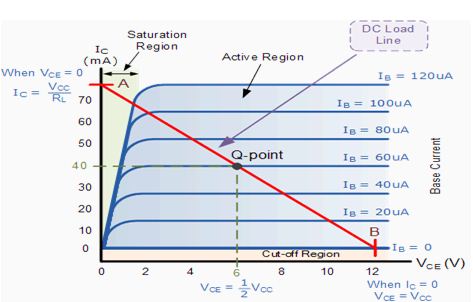
The most important factor to notice is the effect of Vce upon the collector current Ic when Vce is greater than about 1.0 volts. We can see that Ic is largely unaffected by changes in Vce above this value and instead it is almost entirely controlled by the base current, Ib. When this happens we can say then that the output circuit represents that of a "Constant Current Source". It can also be seen from the common emitter circuit above that the emitter current Ie is the sum of the collector current, Ic and the base current, Ib, added together so we can also say that Ie = Ic + Ib for the common emitter (CE) configuration.
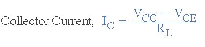
By using the output characteristics curves in our example above and also Ohm´s Law, the current flowing through the load resistor, (RL), is equal to the collector current, Ic entering the transistor which inturn corresponds to the supply voltage, (Vcc) minus the voltage drop between the collector and the emitter terminals, (Vce) and is given as:
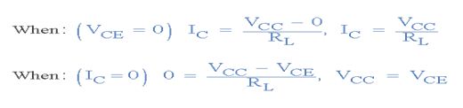
Also, a straight line representing the Dynamic Load Line of the transistor can be drawn directly onto the graph of curves above from the point of "Saturation" ( A ) when Vce = 0 to the point of "Cut-off" ( B ) when Ic = 0 thus giving us the "Operating" or Q-point of the transistor. These two points are joined together by a straight line and any position along this straight line represents the "Active Region" of the transistor. The actual position of the load line on the characteristics curves can be calculated as follows:
Then, the collector or output characteristics curves for Common Emitter NPN Transistors can be used to predict the Collector current, Ic, when given Vce and the Base current, Ib. A Load Line can also be constructed onto the curves to determine a suitable Operating or Q-point which can be set by adjustment of the base current. The slope of this load line is equal to the reciprocal of the load resistance which is given as: -1/RL
Then we can define a NPN Transistor as being normally "OFF" but a small input current and a small positive voltage at its Base (B) relative to its Emitter (E) will turn it "ON" allowing a much large Collector-Emitter current to flow. NPN transistors conduct when Vc is much greater than Ve.
The PNP Transistor
The PNP Transistor is the exact opposite to the NPN Transistor device we looked at in the previous tutorial. Basically, in this type of transistor construction the two diodes are reversed with respect to the NPN type giving a Positive-Negative-Positive configuration, with the arrow which also defines the Emitter terminal this time pointing inwards in the transistor symbol.
Also, all the polarities for a PNP transistor are reversed which means that it "sinks" current into its Base as opposed to the NPN transistor which "sources" current through its Base. The main difference between the two types of transistors is that holes are the more important carriers for PNP transistors, whereas electrons are the important carriers for NPN transistors. Then, PNP transistors use a small base current and a negative base voltage to control a much larger emitter-collector current. In other words for a PNP transistor, the Emitter is more positive with respect to the Base and also with respect to the Collector.
The construction of a "PNP transistor" consists of two P-type semiconductor materials either side of an N-type material as shown below.
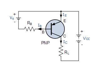
A PNP Transistor Configuration
The construction and terminal voltages for an NPN transistor are shown above. The PNP Transistor has very similar characteristics to their NPN bipolar cousins, except that the polarities (or biasing) of the current and voltage directions are reversed for any one of the possible three configurations looked at in the first tutorial, Common Base, Common Emitter and Common Collector.
PNP Transistor Connections
The voltage between the Base and Emitter ( VBE ), is now negative at the Base and positive at the Emitter because for a PNP transistor, the Base terminal is always biased negative with respect to the Emitter. Also the Emitter supply voltage is positive with respect to the Collector ( VCE ). So for a PNP transistor to conduct the Emitter is always more positive with respect to both the Base and the Collector.
The voltage sources are connected to a PNP transistor are as shown. This time the Emitter is connected to the supply voltage VCC with the load resistor, RL which limits the maximum current flowing through the device connected to the Collector terminal. The Base voltage VB which is biased negative with respect to the Emitter and is connected to the Base resistor RB, which again is used to limit the maximum Base current.
To cause the Base current to flow in a PNP transistor the Base needs to be more negative than the Emitter (current must leave the base) by approx 0.7 volts for a silicon device or 0.3 volts for a germanium device with the formulas used to calculate the Base resistor, Base current or Collector current are the same as those used for an equivalent NPN transistor and is given as.
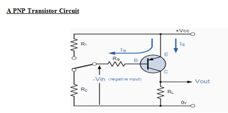
Generally, the PNP transistor can replace NPN transistors in most electronic circuits, the only difference is the polarities of the voltages, and the directions of the current flow. PNP transistors can also be used as switching devices and an example of a PNP transistor switch is shown below.
The Output Characteristics Curves for a PNP transistor look very similar to those for an equivalent NPN transistor except that they are rotated by 180o to take account of the reverse polarity voltages and currents, (the currents flowing out of the Base and Collector in a PNP transistor are negative). The same dynamic load line can be drawn onto the I-V curves to find the PNP transistors operating points..
Last modified: Wednesday, 4 December 2013, 11:11 AM