Site pages
Current course
Participants
General
MODULE 1.
MODULE 2.
MODULE 3.
MODULE 4.
MODULE 5.
MODULE 6.
MODULE 7.
MODULE 8.
MODULE 9.
MODULE 10.
LESSON 13. Common emitter amplifier-practical circuits-phase reversal
Common emitter amplifier
 An amplifier is used to increase the small signal level; i.e. the amplifier is used to get a larger signal output from a small signal input. We will assume a sinusoidal signal at the input of the amplifier. At the output, signal must remain sinusoidal in waveform, with frequency same as that of the input.
To make the transistor work as an amplifier, it is to be biased to operate in the active region, i.e. base-emitter junction is to be forward biased, while base-collector junction to be reversed biased.
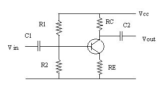
Let us consider the common emitter amplifier circuit using self bias or voltage divider bias as shown in the above Figure.
ISQ is quiescent DC base current
In the absence of input signal, only dc voltage are present in the circuit. This is known as zero-signal or no-signal condition or quiescent condition for the amplifier. The dc collector-emitter voltage, VCE, the dc collector current IC and dc base current IB is the quiescent operating point for the amplifier. On this dc quiescent operating point, we superimpose ac signal by application of ac sinusoidal voltage at the input. Due to this base current varies sinusoidally, as shown in Figure.
Since the transistor is biased to operate in the active region, the output is linearly proportional to the input. The output current i.e. the collector current is β times larger than the input base current in common emitter configuration. Hence the collector current will also vary sinusoidally about its quiescent value, ICQ. The input voltage will also vary sinusoidally as shown in the Figures..
The variations in the collector current and the voltage between collector and emitter due to change in the base current are shown graphically with the help of load line in .The collector current varies above and below its Q point value in-phase with the base current, and the collector-to-emitter voltage varies above and below its Q point value 180° out-of-phase with the base voltage. When one cycle of input is completed, one cycle of output will also be completed. This means the frequency of output sinusoidal is the same as the frequency of input sinusoid. Thus in the amplification process, frequency of the output signal does not change, only the magnitude of the output is larger than that of the input.
Common Emitter Amplifier Circuit
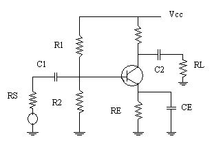
Practical common emitter amplifier circuit
The above figure shows the practical circuit of common emitter transistor amplifier. It consists of different circuit component. The functions of these components are as follows:
- Biasing Circuit
The resistances R1, R2 and RE forms the voltage divider biasing circuit for the CE amplifier. It sets the proper operating point for the CE amplifier.
- Input Capacitor C1
This capacitor couples the signal to the base of the transistor. It blocks any dc component present in the signal and passes only ac signal for amplification. Because of this biasing conditions are maintained constant.
3. Emitter Bypass Capacitor CE
An emitter bypass capacitor CE is connected in parallel with the emitter resistance, RE to provide a low resistance path to the amplified ac signal. If it is not inserted, the amplified ac signal passing through RE will cause a voltage drop across it. This will reduce the output voltage, reducing the gain of the amplifier.
- Output Coupling Capacitor C2
The coupling capacitor C2 couples the output of the amplifier to the load or to the next stage of the amplifier. It blocks dc and passes only ac part of the amplified signal.
Need for C1, C2 and CE
We know that, the impedance of capacitor is given as
XC = ![]()
Thus, at signal frequencies all the capacitors have extremely small impedance and it can be treated as an ac short circuit. For bias / dc conditions of the transistor all the capacitors act as a dc open circuit. With this knowledge we will see the importance of C1, C2 and CE.
Consider that the signal source is connected directly to the base of the transistor as shown in the following figure. Looking at the Figure, we can immediately notice that source resistance RS is in parallel with R2. This will reduce the bias voltage at the transistor base and, consequently alter the collector current, which is not desired. Similarly, by connecting RL directly, the
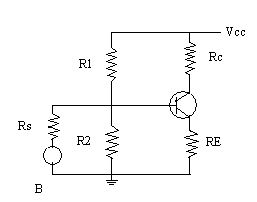
dc levels of VC and VEC will change. To avoid this and maintain this stability of bias condition coupling capacitors are connected. As mentioned earlier, coupling capacitors act as open circuits to dc, maintain stable biasing conditions even after connection of RS and RL. Another advantages of connecting C1 is that any dc component in the signal is opposed and only ac signal is routed to the transistor amplifier.
The emitter resistance RE is one of the component which provides bias stabilization. But it also reduces the voltage swing at the output. The emitter bypass capacitor CE provides a low reactance path to the amplified a.c. signal increasing the output voltage swing.
For the proper operation of the circuit, polarities of the capacitors must be connected correctly. The curve bar which indicates negative terminal must always be connected at a dc voltage level lower than (or equal to) the dc level of the positive terminal (straight bar). For example, C1 in Fig. 1.4 has its negative terminal at dc ground level, because it is grounded through the signal source resistance RS. The positive terminal of C1 is at + VB with respect to ground.
Phase Reversal
The phase relationship between the input and output voltages can be determined by considering the effect of a positive half cycle and negative half cycle separately. Consider the positive half cycle of input signal in which terminal A is positive w.r.t B. Due to this, two voltages, ac and dc will be adding each other, increasing forward bias on base emitter junction. This increases base current. The collector current is β times the base current, hence the collector current will also increase. This increases the voltage drop across RC. Since VC = VCC – ICRC, the increases in IC results in a drop in collector voltage VC, as VCC is constant. Thus, as Vi increases in a positive direction, Vo goes in a negative direction and we get negative half cycle of output voltage for positive half cycle at the input.
In the negative half cycle of input, in which terminal A becomes negative w.r.t. terminal B, the ac and dc voltages will oppose each other, reducing forward bias on base-emitter p-n junction. This reduces base current. Accordingly collector current and drop across RC both reduce, increasing the output voltage. Thus, we get positive half cycle at the output for negative half cycle at the input. Therefore, we can say that there is a phase shift of 180° between input and output voltages for a common emitter amplifier.
Last modified: Thursday, 5 December 2013, 6:50 AM