Site pages
Current course
Participants
General
MODULE 1.
MODULE 2.
MODULE 3.
MODULE 4.
MODULE 5.
MODULE 6.
MODULE 7.
MODULE 8.
MODULE 9.
MODULE 10.
MODULE 11.
MODULE 12.
MODULE 13.
MODULE 14.
MODULE 15.
MODULE 16.
MODULE 17.
MODULE 18.
MODULE 19.
LESSON 10. Amplifiers-general characteristics-classification-Common Emitter amplifier-characteristics-Common Collector amplifier-characteristics.
AMPLIFIER:
-
The important function of an amplifier is the amplification.
-
Circuit that increases the amplitude of the weak signals.
-
The important parameters of an amplifier are input impedance, output impedance, current gain and voltage gain.
A good design of an amplifier circuit must possess high input impedance, low output impedance and high current gain.
-
Constitute an essential part of radio, television and communication devices.
-
In discrete circuits, bipolar JFET, FET is used as amplifying element.
General Characteristics of Amplifier
The amplifier is a two port network having two input terminals and two output terminals, as shown in Fig. 10.1.
Figure 10.1.Two port network of transistorized amplifier
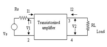
The signal to be amplified is applied to the input terminals and the load is connected to the output terminals. The amplified signal output is available across the load RL. One of the input and output terminals are made generally common, i.e. a straight through connection. The signal to be amplified may be an ac or dc voltage. However we will assume the signal to be an a.c. signal so that the input and output voltages are sinusoidal, at some fixed or variable frequency
The signal is a low level voltage such as obtained from a microphone, tape head, or a transducer. The output load may be a loudspeaker in an audio amplifier, a motor in a servo amplifier, a relay in control application, etc. In any case, the output of the amplifier is an enlarged version of the input. To amplify means to increase the amplitude of, raise the level of, or magnify input. Note that in the amplification process, the frequencies of the input and output signals are exactly identical. If not, there is “ distortion” present in the amplifier. Then the signal is not faithfully reproduced at the output.
The amplifier is constructed using transistors. For their operation as an amplifier, transistors requires proper d.c. biasing. The necessary d.c. voltage is provided by a battery (usually a dry battery) or a d.c. source resulting from a rectifier and filter combination. In this case, the amplifier operates from 230 V,50 Hz a.c. mains supply. Very often, many amplifiers have the facility to operate from a.c. mains or battery.
Referring to Fig. 10.1,
VS : is the signal voltage,
RS : is the internal resistance of the source,
V1 : is the actual input voltage to the amplifier,
I1 : is the input current to the amplifier,
V2 : is the output voltage across the load RL,
I2 : is the output current flowing through the load RL.
The ratio of V1 to I1 is called input resistance, Ri , of the amplifier.
Ri =![]()
V2 is the output voltage across the load RL, and I2 is the output current flowing through the load RL. Ro is the output (or internal) resistance of the amplifier.
The ratio of output current to input current is called current gain, AI, of the amplifier.
Current gain, AI =![]()
The ratio of output voltage to input voltage is called voltage gain, AV =![]()
The ratio of signal power delivered to the load to the signal power at the input of the amplifier is the power gain.
Power gain, 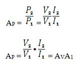
An amplifier may or may not exhibit both a voltage and a current gain, but in general will show a power gain. However, whether voltage or power gain is more important depends upon the application. The amplifier, in which voltage gain is more important than the power gain, is called a voltage amplifier, while in which power gain is more important than voltage gain is known as power amplifier.
CLASSIFICATION:
Based on transistor configuration:
a. Common emitter amplifier.
b. Common collector amplifier.
c. Common base amplifier.
SINGLE STAGE AMPLIFIERS:
Single stage amplifiers have only one amplifying device, say BJT in CE, CC, or CB configuration or FET in CS, CD, or CS configuration.
Based on the active device amplifiers are classified as:
- BJT Amplifier.
- FET Amplifier.
Common Emitter Amplifier:
- NPN Transistor, emitter base junction forward biased by power supply Vbb, collector base junction is reverse biased by power supply Vcc.
- Transistor is active zone throughout its operation.
- Input signal is applied to base emitter circuit and output signal is taken from the collector emitter circuit,
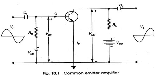
C1, C2 are the coupling capacitors to provide DC isolation at the input and output of the amplifier.
+ Ve input signal is converted into – Ve going output signal,
Ie. 180` phase shift.
Characteristics of CE Amplifier:
-
Large current gain Ai.
-
Large voltage gain Av.
-
Large power gain Ap = Ai. Av.
-
Voltage phase shift of 180º.
-
Moderate input impedance.
-
Moderate output impedance.
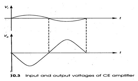
Input & Output voltages of CE Amplifiers:
Common Collector (CC) Amplifier:
NPN Transistor, emitter base junction forward biased by power supply Vee, collector base junction is reverse biased by power supply Vcc,
Transistor is active zone throughout its operation.
Input signal is applied to base collector circuit and output signal is taken from the emitter collector circuit,
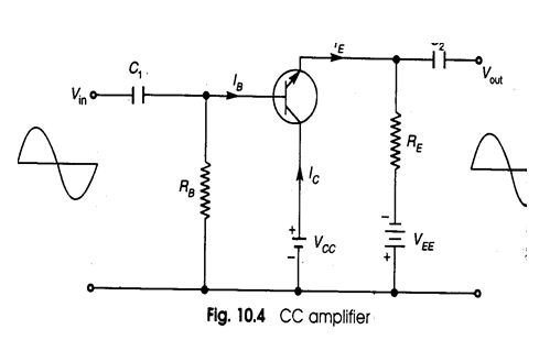
- C1, C2 are the coupling capacitors to provide DC isolation at the input and output of the amplifier.
+ Ve input signal is converted into + ve going output signal,
Hence CC amplifier is also called as emitter follower.
Characteristics of CC Amplifier:
- High current gain
- Voltage gain approximately unity
- Power gain approximately equal to current gain
- No current or voltage phase shift
- Large input impedance
- Small output impedance
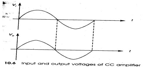
Input & Output voltages of CC Amplifier:
Last modified: Wednesday, 4 December 2013, 11:13 AM