Site pages
Current course
Participants
General
MODULE 1.
MODULE 2.
MODULE 3.
MODULE 4.
MODULE 5.
MODULE 6.
MODULE 7.
MODULE 8.
MODULE 9.
MODULE 10.
MODULE 11.
MODULE 12.
MODULE 13.
MODULE 14.
MODULE 15.
MODULE 16.
MODULE 17.
MODULE 18.
MODULE 19.
LESSON 15. Integrated circuit-advantages-classification-types of amplifiers-operational amplifiers-characteristics of ideal operational amplifier
Integrated Circuit is an Improvement in the characterisation and minimisation of solid state devices and components (transistors, diodes etc.,)
It is a single – crystal chip of silicon, containing both active (transistors and diodes) and passive (resistors and capacitors) elements and their interconnections
Advantages of Integrated Circuit
-
Extremely small in size
-
Low power consumption
-
Reliability
-
Reduced cost
-
Very small weight
-
Easy replacement
Classification of ICs Based on type of signal processed
-
Linear or Analog ICs – Op-amps, voltage regulators, voltage comparators, timers etc., - signals represented by continuous or analog variables
-
Digital ICs – logic gates, counters, digital clock chips, calculator chips, memory chips, memory processors etc., - represented by binary digits and involve logic and memory
Classification of ICs Based on fabrication process
-
Monolithic ICs
-
Hybrid ICs
Types of amplifiers
-
Operational Amplifier
-
Buffer amplifier
-
Differential amplifier
-
Instrumentation amplifier
Operational Amplifiers
The operational amplifier is a direct-coupled high gain (negative feedback) amplifier. It can amplify signals having frequency ranging from 0HZ to MHZ. It is used to perform a wide variety of linear functions and also some non-linear functions. Therefore it is also referred to as the basic linear integrated circuit. An operational amplifier is so named because it was originally designed to perform mathematical operations like subtraction, summation, differentiation, integration and multiplication etc., in analog computer.
Basic operational Amplifiers
Fig 15.1 shows the schematic diagram operational amplifier. It contains tow inputs called as inverting and non-inverting input.
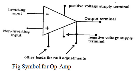
1. Inverting input
The signal given to this input is always inverted at the output. i.e. When positive supply is given, the output will be negative. When negative supply is given, the output will be positive.
2. Non-inverting input
When the signal is given to this non-inverting input terminal, output is available without any change in sign.
Characteristics Ideal operational amplifier:
1. Input resistance Ri = α
2. Output resistance R0 = O
3 Voltage gain VA = α
4, Bandwidth = α
5. Perfect balance V0 = O when V1 = V2
6. Characteristics do not drift with temperature.
Block diagram of an Op-amp.
An integrated amplifier is a four stage cascaded amplifier as shown in Fig. 15.2
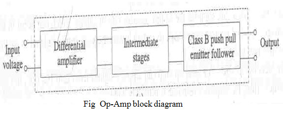
The first stage is a differential amplifier with a double ended output. This stage provides the maximum voltage gain. The second stage is also a differential amplifier. But is has single ended output driver. Because of this stage, the output voltage is zero when the input is zero. And also output resistance is very low and hence it supplies large output voltage or current.
Output resistance (Ro)
This is the effective resistance between the two inputs when it is operated open loop system.
Differential input resistance (Ri)
This is the effective resistance between the two inputs when it is operated in open loop system.
Differential voltage gain (Ad)
This is the ratio of change in output voltage to the corresponding change in differential input voltage.
Slew rate (Sr)
Slew rate is defined as the maximum rate of change of output voltage, when the input is over driven (at large input signal condition). Its unit is volt/micro second.
Input offset voltage (Vor)
This is the differential DC input voltage required to provide zero output voltage with zero input signal. It is usually represented at room temperature and at rated power supply voltage.
Common mode voltage gain (Ac)
This is the ratio of the output signal voltage to the signal voltage applied to the two input terminals in parallel.
Common Mode Rejection Ratio (CMRR)
In an ideal op-amp the common mode input signal is rejected and the output is zero. But real op-amps have a common mode gain Ao.
The common mode rejection ratio is the ratio of the differential mode voltage gain Ad to the common mode voltage gain Ac
CMRR = Ad / Ac
Large value of a CMRR is always preferred. It is expressed in decibels.
Open loop voltage gain: (A)
This is the effective output signal voltage to differential input signal voltage without feed back.
Pin details of Op-Amp
The pin details of the p-Amp is shown in fig.15.3.
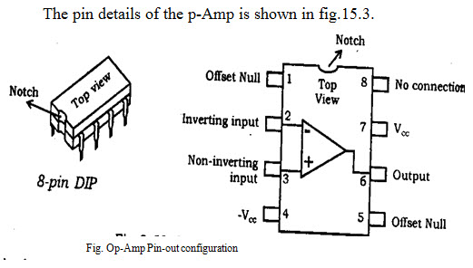
The top pin on the left side of the notch indicates Pin 1. The pin number 2 is inverting input terminal and 3 is non-inverting input terminal. Pin 6 is output terminal. A d.c. voltage or a.c. signal placed on the inverting input will be 180o out of phase at the output. A d.c. voltage or a.c. signal placed on the non-inverting input will be inphase at the output. Pins 7 and 4 are the power supply terminals. Terminals 1 and 5 are used for null adjustment. Null adjustment pins are used to null the output voltage when equal voltages are applied to the input terminals for perfect balance. Pin 8 indicates no connection.
Last modified: Thursday, 5 December 2013, 7:32 AM