Site pages
Current course
Participants
General
MODULE 1.
MODULE 2.
MODULE 3.
MODULE 4.
MODULE 5.
MODULE 6.
MODULE 7.
MODULE 8.
MODULE 9.
MODULE 10.
MODULE 11.
MODULE 12.
MODULE 13.
MODULE 14.
MODULE 15.
MODULE 16.
MODULE 17.
MODULE 18.
MODULE 19.
LESSON 21. Digital to Analog converter- transfer characteristics- conversion techniques. Binary weighted resister DAC-drawback.
Digital to Analog Converter (DAC) and Analog to Digital Converter (ADC)
Introduction
The digital to analog conversion and analog to digital conversion techniques are important tools in the digital data processing systems. The digital to analog conversion technique involves conversion of digital information into equivalent analog information. Digital to analog converts acts as a decoding device since it operates on the output of a digital system. Using analog to digital conversion techniques, the analog information is converted into its equivalent binary number which is in the digital form. In general, the analog to digital converter acts as an encoder. In this chapter, we will discuss various DAC and ADC techniques in details. The discussion of the performance parameters of ADC and DAC is included in the chapter. As the digital to analog conversion is the integral part of an analog to digital conversion, let us discuss first the DAC.
Digital to Analog Converter (DAC)
It is clear from name itself that digital to analog converters are the circuits which convert digital signals into analog converters are very important components inside analog to digital converters. The digital to analog converters (DACs) are also used in many other applications such as cathod ray tube display systems, voice synthesizers, automatic test systems and process control actuators. It is the most important component in computers.
The DAC can perform its conversion in either serial or parallel form depending upon the application in which it is used. For example, process control applications such as bottle filling systems require slow or serial operation, while modern instrumentation such as digital storage oscilloscopes and military weapon systems required very fast or parallel operation.
In general, the input quantity to the DAC is a digital number, the conversion techniques convert the number into corresponding number of units of current, voltage or charge and then these units are added together with an analog summing circuits.
A basic block diagram of commercial DAC is shown in the fig.
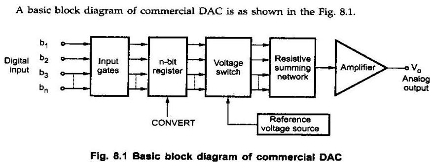 The n-bit digital input number which is to be converted is fed to the n-bit register through the input gates of DAC, upon the execution of CONVERT command. Here b1 to bn are binary digits; either 0 or 1. Note that the register accepts only a digital input during the CONVERT command. This register holds this inputed digital number constant till next CONVERT command is received. The outputs of the register are fed to the voltage switches that provide two possible outputs either 0 V or voltage equal to the value of precision reference voltage source. Thus these switches are exactly similar to the single pole double through (SPDT) switches. The voltage switches are realized in the form of transistor switches. These switches provide access to the resistive summing network which converts each bit into its weighted current value and then adds to get a total current. The total value is then fed to an amplifier which performs current to voltage conversion and output scaling.
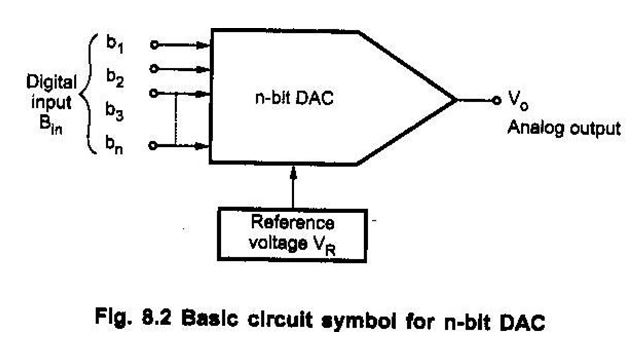
In general, a DAC accepts an n – bit digital input word say b1 , b2 , b3 ,…… bn in binary format and produces an analog output signal Vout proportional to input digital signal Bin. Bin is defined as n-bit digital word given by
Bin = b1 2-1 + b2 2-2 + b3 2-3 + ………. + bn 2-n ….(1)
Note that each digital input can be represented by an electrical signal representing either logic 1 and logic 0. Also b1 is defined as most significant bit (MSB), while bn is defined as least significant bit (LSB). A basic circuit symbol for n-bit D/A converter is as shown in fig.
The relationship between digital input word Bin, analog output Vo and reference voltage VR is given by,
Vo = VR . Bin = VR (b1 2-1 + b2 2-2 + b3 2-3 + ………. + bn 2-n ) …..(2)
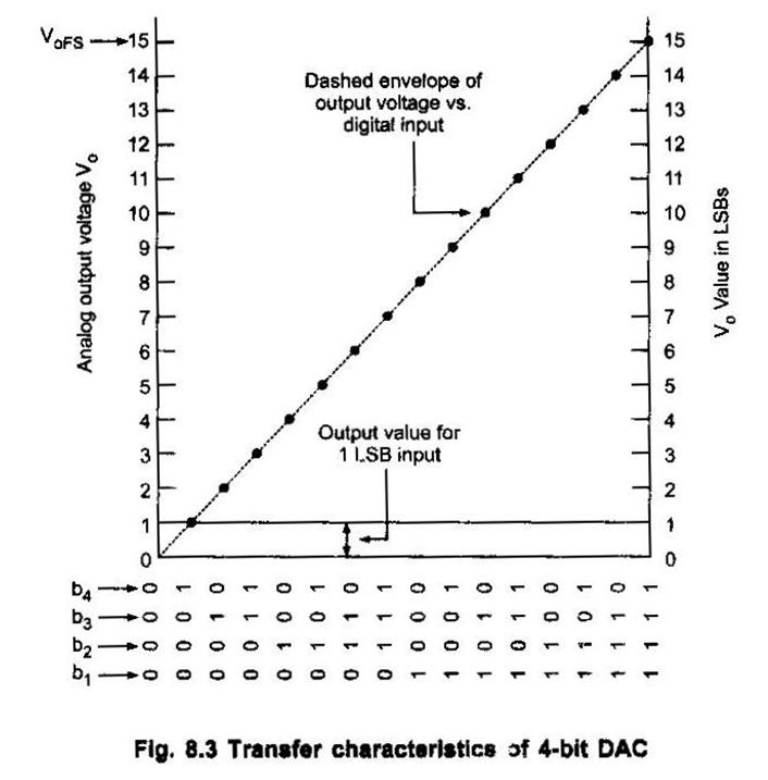
Transfer Characteristic of DAC
The transfer characteristics of 4-bit DAC is shown in fig. In the transfer characteristic, analog output voltage Vo is plotted against all 16 possible inputs.
Digital to Analog Conversion Techniques
There are mainly two techniques used for digital to analog conversion.
- Binary weighted resistor DAC
- R/2R ladder DAC
In these techniques, the shunt resistors are used to generate n binary weighted currents. These currents are added according to switch positions controlled by the digital input and then converted into voltage to give analog voltage equivalent to the digital input. Therefore, such digital to analog converters are called current driven DACs.
Binary Weighted Resistor DAC
The binary weighted resistor DAC uses an op-amp to sum n binary weighted currents derived from a reference voltage VR via current scaling resistors 2R, 4R, 8R, ….2n R, as shown in fig.
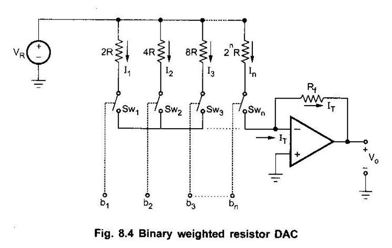
As shown in fig. switch positions are controlled by the digital inputs. When digital input is logic 1, it connects the corresponding resistance to the reference voltage VR ; otherwise it leaves resistor open. Therefore,
VR
For ON-Switch, I = ------- and
R
For OFF – Switch I = 0
Here operational amplifier is used as a summing amplifier. Due to high input impedance of op-amp, summing current will flow through Rf. Hence the total current through Rf can be given as
IT = I1 + I2 + I3 + …….. In
The output voltage is the voltage across Rf and it is given as
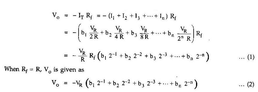
The equation (1) indicates that the analog output voltage is proportional to the input digital word.
The simplicity of the binary weighted DAC is offset by drawbacks associated with it.
Drawbacks
wide range of resistor values are required. For 8-bit DAC, the resistors required are 21 R, 22 R, 23 R , …… and 28 R. Therefore the largest resistor is 128 times the smallest one.
This wide range of resistor values has restrictions on both, higher and lower ends. It is impracticable to fabricate large values of resistor in IC and voltage drop across such a large resistor due to the bias current also affects the accuracy. For smaller values of resistors, the loading effect may occur.
The finite resistance of the switches disturbs the binary-weighted relationship among the various currents, particularly in the most significant bit positions, where the current setting resistance are smaller.
All these drawbacks, especially the requirement of wide range of resistors restricts the use of binary weighted resistor DACs below 8 bits.
Last modified: Thursday, 5 December 2013, 7:48 AM