Site pages
Current course
Participants
General
MODULE 1.
MODULE 2.
MODULE 3.
MODULE 4.
MODULE 5.
MODULE 6.
MODULE 7.
MODULE 8.
MODULE 9.
MODULE 10.
MODULE 11.
MODULE 12.
MODULE 13.
MODULE 14.
MODULE 15.
MODULE 16.
MODULE 17.
MODULE 18.
MODULE 19.
LESSON 23. Analog to digital converter-transfer characteristics-conversion techniques-successive approximate ADC.
Analog to Digital Converters (ADC)
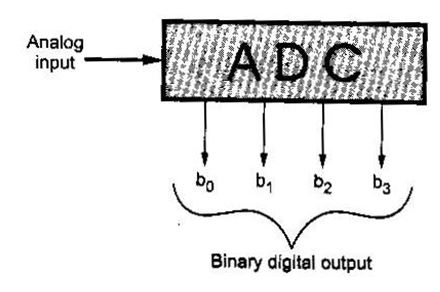
The analog to digital conversion is a quantizing process where by an analog signal is converted into an equivalent binary word. The fig. shows the symbol for A/D converter.
Transfer Characteristics of ADC
The graph of output plotted against the input is called transfer characteristics. Thus transfer characteristics of ADC is the graph of digital output against the analog input. The fig. shows the transfer characteristics of a 3-bit ADC.
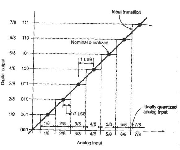
The transfer characteristics shows 23 (as 3 bit) discrete output states i.e., from binary 0002 to 1112. The suffix 2 indicates binary nature of the output. The each step is being 1/8 V apart.From this transfer characteristics, we can define following performance parameters of ADC.
Resolution
The resolution of ADC is defined as the number of different digital outputs states which can be provided by ADC. Thus for a n bit ADC.
resolution = 2 n ….. (1)
Resolution is also called as the ratio of a change in value of input voltage, Vi , needed to change the digital output by 1 LSB. If the full scale input voltage required to cause a digital output of all 1’s is ViFS , then resolution can be given as
ViFS
resolution = ------------- …..(2)
2n - 1
Quantization Error
The fig. shows that the binary output is 011 for all values of Vi between ¼ and ½ V. There is an unavoidable uncertainly about the exact value of Vi when the output is 011. This uncertainly is specified as quantitization error. Its value is ± ½ LSB.
It is given as,
ViFS
Q E = ------------- …(3)
(2n - 1) 2
Increasing the number of bits results in a finer resolution and a smaller quantization error.
Conversion Time
It is an important parameter for ADC. It is defined as the total time required to convert an analog signal into its digital output. It depends on the conversion technique used and the propagation delay of circuit components.
Example:
An 8-bit ADC outputs all 1’s when Vi = 5.1 V. Find it’s a) Resolution and
b) Digital output when Vi = 1.28 V.
Solution:
a) From equation (1) we have,
resolution = 28 = 256
and from equation (2) we have,
5.1 V
resolution = -------------
28 – 1
= 20 mV/LSB
Therefore, we can say that to change output by 1 LSB we have to change input by 20 mV.
b) For 1.28 V analog input, digital output can be calculated as,
1.28 V
D = -------------------- = 64 LSBs
20 m V / LSB
The binary equivalent of 64 is 0100 00002
Example:
Calculate the quantizing error for 12-bit ADC with full scale input voltage 4.095 V.
Solution
From equation (3) get
4.095
QE = ------------------
(212 - 1) x 2
4.095
= ------------------ = 0.5 mV
(4096 - 1) x 2
Analog to Digital conversion Techniques
Analog to digital converters are classified into two general groups based on the conversion techniques. One technique involves comparing a given analog signal with the internally generated reference voltages. This group includes successive approximation, flash, delta modulated (DM), adaptive delta modulated and flash type converters. The another technique involves changing an analog signal into time or frequency and comparing these new parameters against known values. This group includes integrator converters and voltage-to-frequency converters.
Types of ADCs using various conversion techniques:
Single ramp or single slope
Dual slope
Successive approximation
Flash
Delta Modulation
Adaptive delta modulation
Successive Approximation ADC
In this technique, the basic idea is to adjust the DAC’s input code such that its output us within ± ½ LSB of the analog input Vi to be A/D converted. The code that achieves this represents the desired ADC output.
The successive approximation method uses very efficient code searching strategy called binary search. It completes searching process for n-bit conversion in just n clock periods.
Fig. shows the block diagram of successive approximation ADC. It consists of a DAC, a comparator and a successive approximation register (SAR).
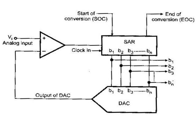
The external clock input sets the internal timing parameters. The control signal start of conversion (SOC) initiates an A/D conversion process and end of conversion signal is activated when the conversion is completed.
Operation:
The searching code process in successive approximation method is similar to weighing an unknown material with a balance scale and a set of standard weights. Let us assume that we have 1 kg, 2 kg and 4 kg weights (SAR) plus a balance scale (comparator and DAC). Now we will see the successive approximation analogy for 3-bit ADC.
The analog voltage Vin is applied at one input of comparator. On receiving start of conversion signal (SOC) successive approximation register sets 3-bit binary code 1002 (b2 = 1) as an input of DAC. This is similar process of placing the unknown weight on one platform of the balance and 4kg weight on the other. The DAC converts the digital word 100 and applies it equivalent analog output at the second input voltage is greater than the analog output of DAC, successive approximation register keeps b2 = 1 and makes b1 = 1 (addition of 2 kg weight to have total 6 kg weight) otherwise it resets b2 = 0 and makes b1 = 1 (replacing 2 kg weight). The same process is replaced for b1 and b0. The status of b0, b1 and b2 bits gives the digital equivalent of the analog input.
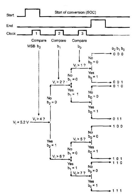
The dark lines in the fig. shows setting and resetting actions of bits for input voltage 5.2 V, on the basis of comparison. It can be seen from the fig. that one clock pulse is required for the successive approximation register to compare each bit. However an additional clock pulse is usually required to reset the register prior to performing a conversion. The time for one analog to digital conversion must depend on both the clock’s period T and number of bits n. It is given as,
TC = T (n +1) ….(1)
Where TC = conversion time
T = clock period
n = number of bits
Example:
An 8-bit successive approximation ADC is driven by a 1 MHz clock. Find its conversion time.
Solution:
f = 1 MHz
1 1
@ T = ----- = ---------------------- = 1 μsec
f 1 x 10 6
n = 8
@TC = T (n + 1) = 1 (8 + 1) = 9 μsec
Last modified: Thursday, 5 December 2013, 7:53 AM