Site pages
Current course
Participants
General
MODULE 1.
MODULE 2.
MODULE 3.
MODULE 4.
MODULE 5.
MODULE 6.
MODULE 7.
MODULE 8.
MODULE 9.
MODULE 10.
MODULE 11.
MODULE 12.
MODULE 13.
MODULE 14.
MODULE 15.
MODULE 16.
MODULE 17.
MODULE 18.
MODULE 19.
LESSON 19. Sequential circuit-Flip flops-types- SR flip flop-JK flip flop-T flip flop.
FLIP FLOPS
Flip-flops are the basic elements for storing information. One latch or flip-flop can store one bit of information. The main difference between latches and flip-flops is that for latches, their outputs are constantly affected by their inputs as long as the enable signal is asserted. In other words, when they are enabled, their content changes immediately when their inputs change. Flip-flops, on the other hand, have their content change only either at the rising or falling edge of the enable signal. This enable signal is usually the controlling clock signal. After the rising or falling edge of the clock, the flip-flop content remains constant even if the input changes.
Flip-flops are the fundamental element of sequential circuits and they are bistable whereas gates are the fundamental element for combinational circuits. Flip-flops are essentially 1-bit storage devices and outputs can be set to store either 0 or 1 depending on the inputs even when the inputs are de-asserted, the outputs retain their prescribed value. Flip-flops have (normally) 2 complimentary outputs and three main types of flip-flop are viz., R-S J-K D-type
SR Latch
The bistable element is able to remember or store one bit of information. However, because it does not have any inputs, we cannot change the information bit that is stored in it. In order to change the information bit, we need to add inputs to the circuit. The simplest way to add inputs is to replace the two inverters with two NAND gates as shown in Figure 4(a). This circuit is called a SR latch. In addition to the two outputs Q and Q', there are two inputs S' and R' for set and reset respectively. Following the convention, the prime in S and R denotes that these inputs are active low. The SR latch can be in one of two states: a set state when Q = 1, or a reset state when Q = 0.
If both S' and R' are asserted, then both Q and Q' are equal to 1 as shown at time t4. If one of the input signals is de-asserted earlier than the other, the latch will end up in the state forced by the signal that was de-asserted later as shown at time t5. At t5, R' is de-asserted first, so the latch goes into the normal set state with Q = 1 and Q' = 0. A problem exists if both S' and R' are de-asserted at exactly the same time as shown at time t6. If both gates have exactly the same delay then they will both output a 0 at exactly the same time. Feeding the zeros back to the gate input will produce a 1, again at exactly the same time, which again will produce a 0, and so on and on. This oscillating behavior, called the critical race, will continue forever.
If the two gates do not have exactly the same delay then the situation is similar to de-asserting one input before the other, and so the latch will go into one state or the other. However, since we do not know which is the faster gate, therefore, we do not know which state the latch will go into. Thus, the latch’s next state is undefined.
In order to avoid this indeterministic behavior, we must make sure that the two inputs are never de-asserted at the same time. Note that both of them can be de-asserted, but just not at the same time. Inpractice, this is guaranteed by not having both of them asserted. Another reason why we do not want both inputs to be asserted is that when they are both asserted, Q is equal to Q', but we usually want Q to be the inverse of Q'.
Bistable Element
Simplest sequential circuit or storage element is a bistable element, which is constructed with two inverters connected sequentially in a loop as shown in Figure 1. It has no inputs and two outputs labeled Q and Q’. Since the circuit has no inputs, we cannot change the values of Q and Q’. However, Q will take on whatever value it happens to be when the circuit is first powered up. Assume that Q = 0 when we switch on the power. Since Q is also the input to the bottom inverter, Q’, therefore, is a 1. A 1 going to the input of the top inverter will produce a 0 at the output Q, which is what we started off with. Similarly, if we start the circuit with Q = 1, we will get Q’ = 0, and again we get a stable situation. A bistable element has memory in the sense that it can remember the content (or state) of the circuit indefinitely. Using the signal Q as the state variable to describe the state of the circuit, we can say that the circuit has two stable states:
Q = 0, and Q = 1; hence the name “bistable.”
An analog analysis of a bistable element, however, reveals that it has three equilibrium points and not two as found from the digital analysis. Assuming again that Q = 1, and we plot the output voltage (Vout1) versus the input voltage (Vin1) of the top inverter.The dotted line shows the operation of the bottom inverter where Vout2 and Vin2 are the output and input voltages respectively for that inverter. Figure 2 shows that there are three intersection points, two of which corresponds to the two stable states of the circuit where Q is either 0 or 1. The third intersection point labeled metastable, is at a voltage that is neither a logical 1 nor a logical 0 voltage. Nevertheless, if we can get the circuit to operate at this voltage, then it can stay at that point indefinitely. Practically, however, we can never operate a circuit at precisely a certain voltage. A slight deviation from the metastable point as cause by noise in the circuit or other stimulants will cause the circuit to go to one of the two stable points. Once at the stable point, a slight deviation, however, will not cause the circuit to go away from the stable point but rather back towards the stable point because of the feedback effect of the circuit.
Flip-Flop Types
There are basically four main types of flip-flops: SR, D, JK, and T. The major differences in these flip-flop types are in the number of inputs they have and how they change state. Each type can have different variations such as active high or low inputs, whether they change state at the rising or falling edge of the clock signal, and whether they have asynchronous inputs or not. The flip-flops can be described fully and uniquely by its logic symbol, characteristic table, characteristic equation, state diagram, or excitation table, and are summarized.
SR Flip-Flop
We can replace the D latches in the D flip-flop of Figure 10(a) with SR latches to get a master-slave SR flipflop shown in Figure 16. Like SR latches, SR flip-flops are useful in control applications where we want to be able to set or reset the data bit. However, unlike SR latches, SR flip-flops change their content only at the active edge of the clock signal. Similar to SR latches, SR flip-flops can enter an undefined state when both inputs are asserted simultaneously.
JK Flip-Flop
JK flip-flops are very similar to SR flip-flops. The J input is just like the S input in that when asserted, it sets the flip-flop. Similarly, the K input is like the R input where it clears the flip-flop when asserted.The only difference is when both inputs are asserted. For the SR flip-flop, the next state is undefined, whereas, for the JK flip-flop, the next state is the inverse of the current state.
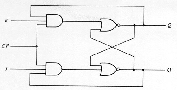
In other words, the JK flip-flop toggles its state when both inputs are asserted. The circuit, truth table and the logic symbol for the JK flip-flop.
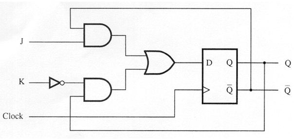
T Flip-Flop
The T flip-flop has one input in addition to the clock. T stands for toggle for the obvious reason. When T is asserted (T = 1), the flip-flop state toggles back and forth, and when T is de-asserted,the flip-flop keeps its current state. The T flip-flop can be constructed using a D flip-flop with the two outputs Q and Q' feedback to the D input through a multiplexer that is controlled by the T input.
Logic Symbol
The logic or graphical symbol describes the flip-flop’s inputs and outputs, the names given to these signals, and whether they are active high or low. All the flip-flops have Q and Q' as their outputs. All of them also have a CLK input. The small triangle at the clock input indicates that the circuit is a flip-flop and so it is triggered by the edge of the clock signal; if there is a circle in front, then it is the falling edge, otherwise, it is the rising edge of the clock.
Characteristic Table
The characteristic table is just the truth table but usually written in a shorter format. For example, compare the characteristic table for the JK flip-flop in Figure 20 with the truth table in Figure 17(b). The truth table, as we have seen, simply lists all possible combinations of the input signals, the current state (or content) of the flip-flop, and the next state that the flip-flop will go to at the next active edge of the clock signal. The characteristic table answers the question of what is the next state when given the inputs and the current state, and is used in the analysis of sequential circuits.
Characteristic Equation
The characteristic equation is the functional Boolean equation that is derived from the characteristic table. This equation formally describes the functional behavior of the flip-flop. Like the characteristic table, it specifies the flipflop’s next state as a function of its current state and inputs. For example, the characteristic equation for the JK flipflop can be derived from the truth table as follows:
Qnext = J'K'Q + JK'Q + JK'Q' + JKQ'
= K'Q(J'+J) + JQ'(K'+K)
= K'Q + JQ'
The characteristic equation can also be obtained from the truth table using the K-map method as follows for the SR flip-flop.
State Diagram
A state diagram is a graph that shows the flip-flop’s operations in terms of how it transitions from one state to another. The nodes are labeled with the states and the directed arcs are labeled with the input signals that cause the transition to go from one state to the next. Figure 21 shows the state diagram for the SR flip-flop. For example, to go from state Q = 0 to the state Q = 1, the two inputs S and R have to be 1 and 0 respectively. Similarly, if the current state is Q = 0 and we want to remain in that state, then SR need to be 00 or 01.
Last modified: Thursday, 5 December 2013, 7:45 AM