Site pages
Current course
Participants
General
MODULE 1.
MODULE 2.
MODULE 3.
MODULE 4.
MODULE 5.
MODULE 6.
MODULE 7.
MODULE 8.
MODULE 9.
MODULE 10.
LESSON 4. Diode circuits-rectifier circuits-Half and full wave rectifier-Bridge rectifier-comparison
Diode Circuits
Diode circuits to be considered perform functions such as rectification, clipping. and clamping. These functions are possible only because of the nonlinear properties of the pn junction diode. The conversion of an ac voltage to a dc voltage, such as for a dc power supply, is called rectification. Clipper diode circuits clip portions of a signal that are above or below some reference level. Clamper circuits shift the entire signal by some dc value, Zener diodes, which operate in the reverse-bias breakdown region, have the advantage that the voltage across the diode in this region is nearly constant over a wide range of currents. Such diodes are used in voltage reference or voltage regulator circuits.
Finally, we look at the circuits of two special diodes: the light-emitting diode (LED) and the photodiode. An LED circuit is used in visual displays, such as the seven-segment numerical display. The photodiode circuit is used to detect the presence or absence of light and convert this information into an electrical signal.
4.1 RECTIFIER CIRCUITS
One important application of diodes is in the design of rectifier circuits. A diode rectifier forms the first stage of a dc power supply as shown in Figure 4.1 below.
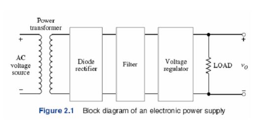
As we will see throughout the text, a dc power supply is required to bias all electronic circuits. The dc output voltage vo will usually be in the range of 3 to 24V depending on the application.
Rectification is the process of converting an ac voltage to one polarity. The diode is useful for this function because of its nonlinear characteristics, that is, current exists for one voltage polarity, but is essentially zero for the opposite polarity. Rectification is classified as half-wave or full-wave, with half-wave being the simplest.
PN Junction diode as rectifier
The process in which alternating voltage or alternating current is converted in to direct voltage or direct current is known as rectification. The device used for this process is called as rectifier. The junction diode has the property of offering low resistance and allowing current to flow through it, in the forward biased condition. This property is used in the process of rectification.
Half wave rectifier
A circuit which rectifies half of the a.c. wave is called half wave rectifier.
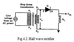
Fig. 4.2 shows the circuit for half wave rectification. The a.c. voltage (VS) to be rectified is obtained across the secondary ends S1 S2 of the transformer. The P-end of the diode D is connected to S1 of the secondary coil of the transformer. The N-end of the diode is connected to the other end S2 of the secondary coil of the transformer, through a load resistance RL. The rectified output voltage Vdc appears across the load resistance RL.
During the positive half cycle of the input a.c. voltage (VS), S1 will be positive and the diode is forward biased and hence it conducts. Therefore, current flows through the circuit and there is a voltage drop across RL. This gives the output voltage as shown in Fig.4.3.
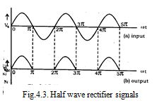
During the negative half cycle of the input a.c. voltage (VS), S1 will be negative and the diode D is reverse biased. Hence the diode does not conduct. No current flows through the circuit and the voltage drop across RL will be zero. Hence no output voltage is obtained. Thus corresponding to an alternating input signal, unidirectional pulsating output is obtained.
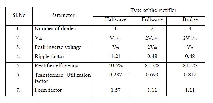
The ratio of d.c. power output to the a.c. power input is known as rectifier efficiency. The efficiency of half wave rectifier is approximately 40.6%.
Full wave rectifier
The circuit which rectifies both half cycles of the a.c. wave is called full wave rectifier.
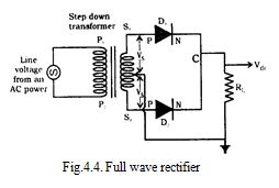
Fig. 4.4 shows the full wave rectifier circuit using two diodes. The a.c. input voltage (VS) to be rectified is obtained from the secondary ends S1 and S2 of the transformer. The P-ends of the diodes D1 and D2 are connected to the secondary ends S1 and S2 of the transformer. The centre tap C is connected to the load resistance, which in turn is connected to the junction of N-ends of the diodes. The rectified output voltage, Vdc appears across the load resistance RL. Because of the centre tap, the circuit is equivalent to two half-wave rectifiers. The upper diode handles the positive half cycle of the secondary voltage, while lower diode handles the negative half cycle of the secondary voltage.
During positive half cycle of the a.c. input, diode D1 is forward biased and it conducts and causes current flow in the load resistance RL. Diode D2 is reverse biased. Therefore, no current flows through it. During the negative half cycle of the a.c. input, diode D2 is forward biased and it conducts. Hence, current flows through RL. During this process, D1 is reverse biased and no current flows through it.
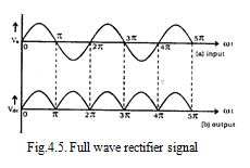
Thus, whether the input signal is positive or negative, current always flows through the load resistance in the same direction. Hence full wave rectification is obtained. Fig. 4.5 shows the output voltage corresponding to the given input voltage. The efficiency of rectification is approximately 81.2%. The efficiency of full wave rectifier is twice that of half wave rectifier.
Bridge rectifier
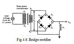
A bridge rectifier is shown in Fig.4.6. There are four diodes D1, D2, D3 and D4 used in the circuit, which are connected to form a network. The input ends A and C of the network are connected to the secondary ends S1 and S2 of the transformer. The output ends B and D are connected to the load resistance RL.
During positive input half cycle of the a.c. voltage, the point A is positive with respect to C. 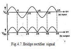 The diodes D1 and D3 are forward biased and conduct, whereas the diodes D2 and D4 are reverse biased and do not conduct. Hence current flows along S1ABDCS2 through RL. During negative half cycle, the point C is positive with respect to A. The diodes D2 and D4 are forward biased and conduct, whereas the diodes D1 and D3 are reverse biased and they do not conduct. Hence current flows along S2CBDAS1 through RL. The same process is repeated for subsequent half cycles. It can be seen that, current flows through RL in the same direction, during both half cycles of the input a.c. signals. The output signal corresponding to the input signal is shown in Fig.4.7. The efficiency of the bridge rectifier is approximately 81.2% Because the full secondary voltage is applied to the conducting diodes in series with the load resistance, the load voltage is twice that of the full-wave rectifier.
Advantages of bridge rectifier
-
Centre tap on the secondary of the transformer is not necessary
-
Smaller transformer can be used
-
It is suited for high voltage applications
Some of the important terminologies related to Rectifier are:
Cut in or threshold voltage (Vr): It is the forward voltage in a diode under forward bias condition, below which the current is very small. It is 0.3V foir Germanium and 0.7V for Silicon. Vi = Vm Sinwt, where Vm >>Vr
Rectifier Efficiency (h): The ratio of dc output to ac input power is known as rectifier efficiency (h) h = (dc output power)/(ac input power)
Ripple Factor (t): The ratio of rms value of ac component to the dc component in the output is known as Ripple Factor (t)
Ripple Factor (t) = (rms value of ac component)/dc component)
Peak Inverse Value (PIV): It is defined as the maximum reverse voltage that a diode can withstand without destroying the junction. For half wave rectifier PIV = Vm.
Transformer Utilization factor (TUF):
TUF = (dc power delivered to the load)/(ac rating of the transformer secondary)
= Pdc/Pac rated
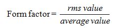
Form factor:
Peak factor:
![]()
Comparison of rectifiers
Last modified: Wednesday, 4 December 2013, 10:42 AM