Site pages
Current course
Participants
General
MODULE 1. Magnetism
MODULE 2. Particle Physics
MODULE 3. Modern Physics
MODULE 4. Semicoductor Physics
MODULE 5. Superconductivty
MODULE 6. Optics
LESSON 18. Band Theory of Solid
Band theory of solids
In an atom, the electrons in inner shells are tightly bound to the nucleus while the electrons in the outermost shell (i.e the valance electron) are loosely bound to the nucleus.
During the formation of a solid, a large number of atoms are brought very close together; the energy levels of these valence electrons are affected most.
The energies of inner shell electrons are not affected much.
The band formed by a series of energy levels containing the valence electrons is called the Valence Band (VB).
It is highest occupied energy band.
It may be completely filled or partially filled with electrons.
The next higher permitted energy band is called the Conduction Band (CB).
It may also be defined as the lowest unfilled permitted energy band.
It may be empty or partially filled with electrons.
The electrons can move freely in the conduction band and hence the electrons in conduction band are called conduction electrons.
The energy gap between the VB and CB is called the Forbidden Energy Gap or Forbidden Band.
This band is formed by a series of non-permitted energy levels above the top of valence band and below the bottom of the conduction band.
It is denoted by Eg and is the amount of energy to be supplied to the electron in VB to get excited into the CB.
When an electron gains sufficient energy, it is ejected from the valence band. Because of this, a covalent bond is broken and a vacancy for electron, called Hole, is generated.
It is supposed to behave as a positive charge.
This Hole can travel to the adjacent atom by acquiring an electron from an atom.
When an electron is captured by a Hole, the covalent bond is again re-established.
Thus conduction electrons are found in and above freely in the conduction band. The Holes exist in and move in the valence band.
Distinction between Metal, Insulator and Semiconductor
-
There are many energy bands in solids as there are energy levels in parent atom.
-
The electrical conduction properties of solids are concerned, only the valance band and conduction band energies of the electron are considered.
-
Completely filled bands and completely empty bands do not contribute to electrical conduction.
-
The electrons in the innermost filled shell do not take part in conduction process.
-
The electrons in conduction band are free and move easily under an electric field.
-
The electrons in valance band are attached to the lattice and are not free to move
-
If they acquire sufficient energy to cross the forbidden gap Eg, they occupy the conduction band states are available for conduction.
-
On the basis of the band theory, solids are classified into three categories;
-
Insulator
-
Semiconductor
-
Conductor
-
Insulator
These are those materials in which the valence electrons are bound very tightly to their parent atoms.
Hence very large electric field is needed to remove them from attraction of nuclei.
The band picture if insulator is shown in Fig.
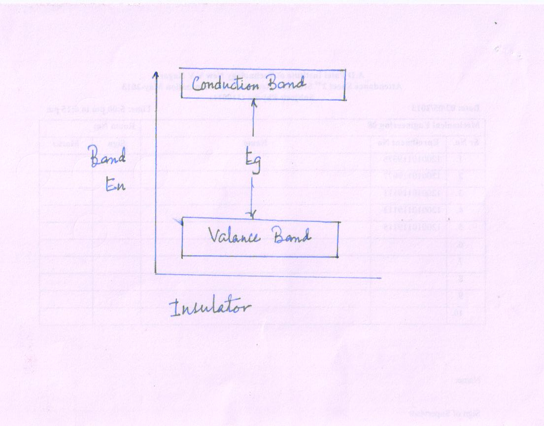 Features of Insulator
A full valance band
An empty conduction band
A large band gap Eg; = 5-10 eV
Very high resistivity of order of 109 Ω cm
Some samples at high temperature and under sufficient electric field, some electrons may move from valance band to conduction band. Hence insulator shows small conductivity at high temperature.
e.g. diamond and glass
Semiconductors
A semiconducting material has electrical properties between those of insulators and good conductors.
The band diagram of semiconductor is shown in Fig.
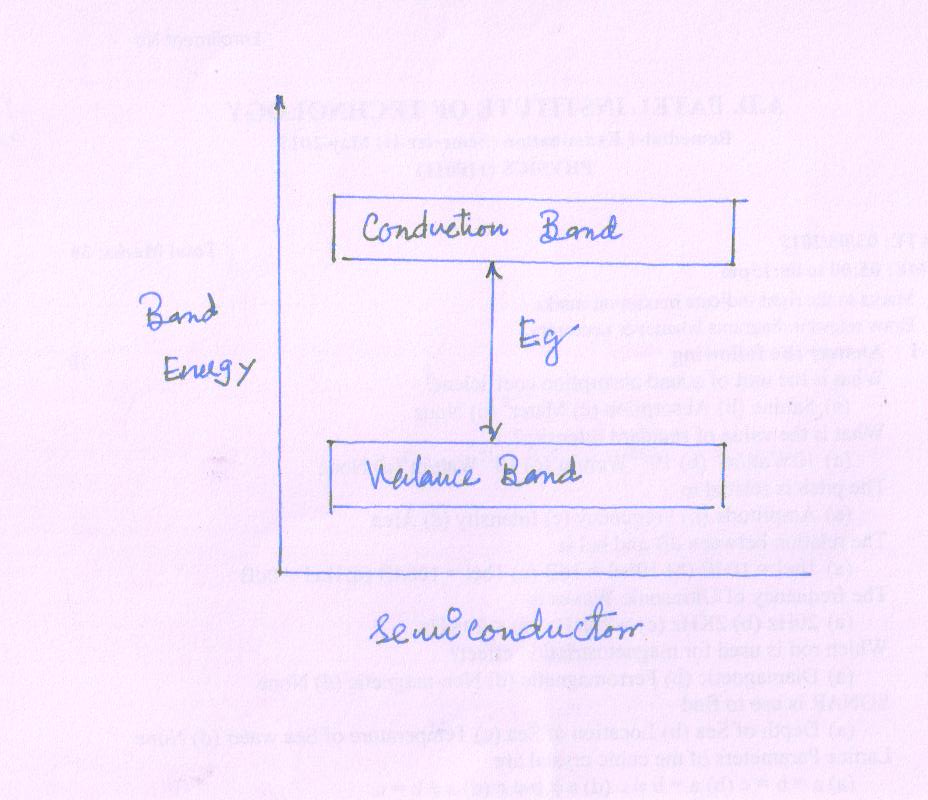
Features of Semiconductors
-
Almost empty conduction band and filled valance band with a very narrow energy gap Eg = 1 eV
-
At 0K, the valance band is completely filled and the conduction band is empty.
-
As temperature increases the electron in valance band acquire enough energy to cross the small energy gap and move to CB. Thus the conductivity of semiconductors increases with temperature.
-
The electron moving to CB leave behind positive holes in VB . Hence, semiconductor current is the sum of electron and hole current flowing in opposite direction.
-
The resistivity varies from to 10-12 to 109 Ω cm
e.g. Ge = Eg = 0.7 eV and Si = Eg = 1.1 eV
Conductors
-
The conductors have a large number of free electrons available for electrical conduction.
-
Conductors may be defined as solids characterized by a single energy band called conduction band, which is partially filled at any temperature.
-
Alternatively, a conductor as a solid, in which the conduction and valance bands overlap and there is no energy gap between the two bands
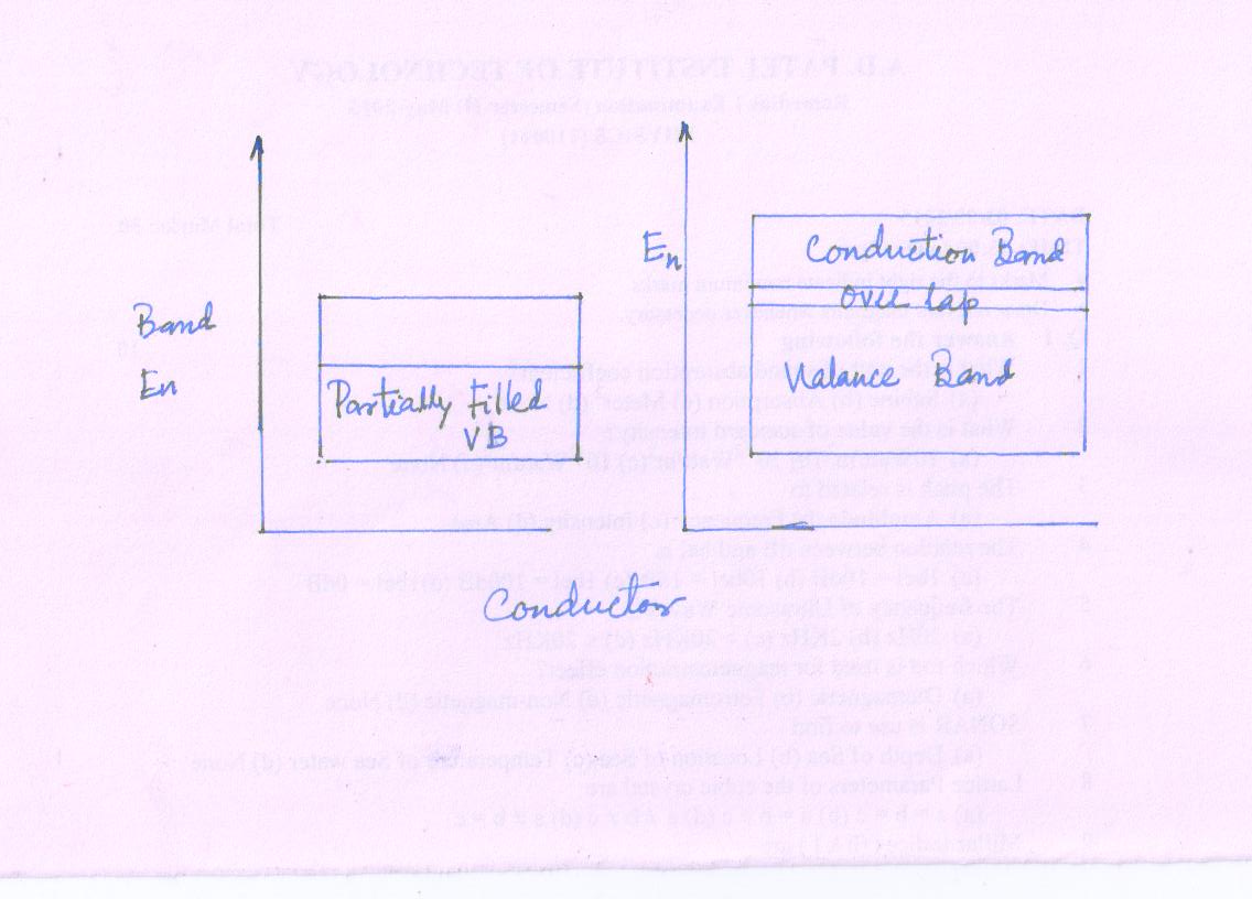 As there is no forbidden gap, there is no structure to establish holes.
- The total current is simply due to the flow of electrons.
e.g. Lithium, Beryllium, Sodium
Last modified: Wednesday, 1 January 2014, 8:20 AM