Site pages
Current course
Participants
General
MODULE 1. Magnetism
MODULE 2. Particle Physics
MODULE 3. Modern Physics
MODULE 4. Semicoductor Physics
MODULE 5. Superconductivty
MODULE 6. Optics
LESSON 19. Classification of Solids & Type of Semiconductor
Type of Semiconductor
It has been already discussed; a semiconductor is material whose electrical properties lie between those of insulator and conductor.
A semiconductor has almost filled valence band and almost empty conduction band with a very small energy gap between the two.
The semiconductors are of two types:
(i) Pure or Intrinsic Semiconductor
(ii) Doped or extrinsic semiconductor
Pure or Intrinsic Semiconductors
-
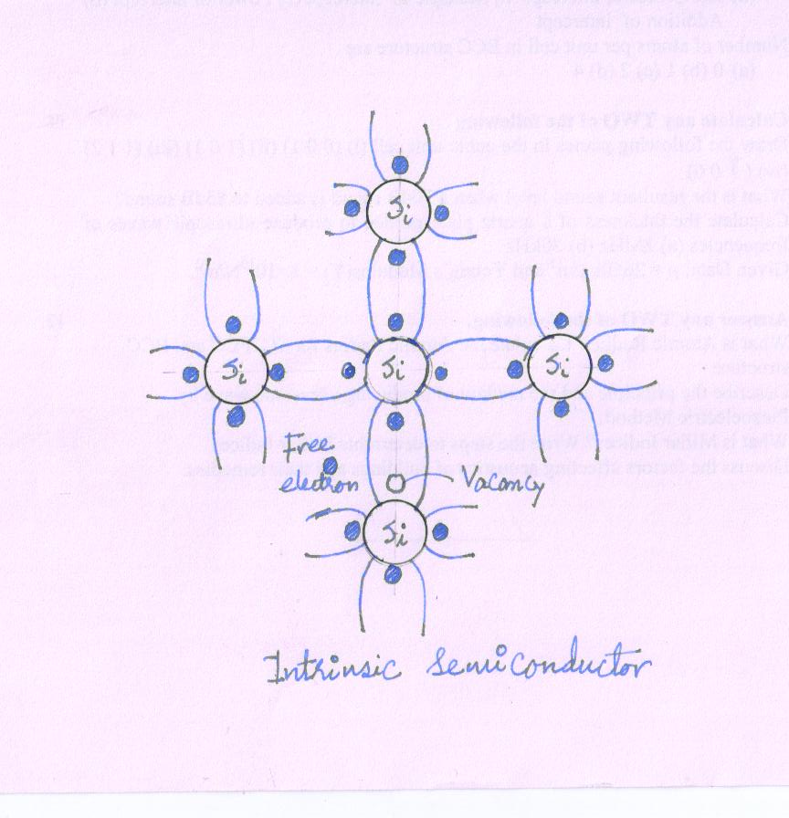
Semiconductor like Ge and Si has crystalline structure. Their atoms are arranged in an ordered array known as the crystal lattice.
-
These materials are tetravalent in nature; with four valence electrons in the outermost shell.
-
The neighboring atoms form covalent bonds by sharing four electrons with each other so as achieved stable structure.
-
A two dimensional structure of Ge crystal lattice is shown in Fig.

-
in which the circles represent atom cores consisting of the nuclei and inner 28 electrons.
-
Each pair of lines represents a covalent bond.
-
The dots represent the valence electrons.
-
The intrinsic semiconductor is the material in its very pure form.
-
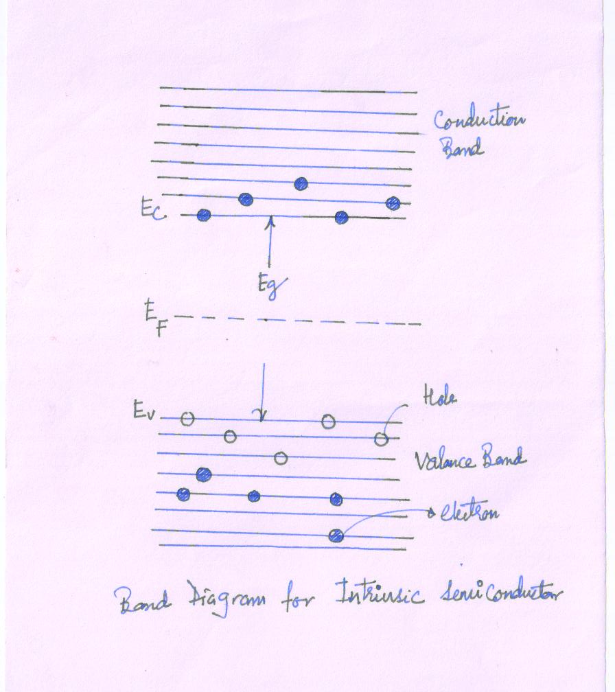
The band diagram of pure semiconductor is shown in Fig.

-
At temperature 0K all the electrons are paired and are contained in the completely filled valence band.
-
No electron is free for conduction band. Hence the conduction band is completely empty.
-
The energy gap between the two bands is small Eg= 0.72 eV for Ge
-
At 0K the energies of this magnitude are usually not acquired by the applied field. Hence the valence band remains full, the conduction band empty and the material behaves as insulator.
-
At room temperature, nearly 300K, some of the valence electrons acquire thermal energy greater than Eg and hence they can jump to the higher conduction band.
-
They now act as free electrons and can move under the influence of small applied field.
-
The absence of electron in the valence band is the Hole.
-
Under the influence of electric field, an electron form the neighboring covalent bond may fill this vacancy i.e. hole moves in a direction opposite to electron motion in valence band.
-
The Hole moves in the same direction as would a positive charge carrier. Hence, in semiconductors there are two types of charge carrier. The total current is the sum of the electrons and hole current.
-
In the intrinsic semiconductor, electrons and holes are generated in pair.
-
At any given temperature, the number of electrons in conduction band and number of holes in valance band are same.
-
With the rise in temperature, more and more electron hole pairs are formed and more charge carriers are available for conduction. Hence the conductivity of intrinsic semiconductors increases with the rise in temperature.
-
The intrinsic semiconductors have low conductivity.
Doped or Extrinsic Semiconductors
Most of the engineering applications of semiconductors involves doped semiconductors with specify impurities rather than the intrinsic material.
Doping is the process of adding a controlled quantity of impurity to intrinsic semiconductors, so as to increase its conductivity. A semiconductor doped with impurity atoms is called an extrinsic semiconductor.
The impurity is added to the melt of Ge or Si , then the crystal is grown in which the impurities are incorporated.
The impurity atoms occupy lattice positions which were occupied by germanium atoms in pure metal.
Two types of extrinsic semiconductors are produced depending upon the group impurity atom.
N -Type of semiconductor
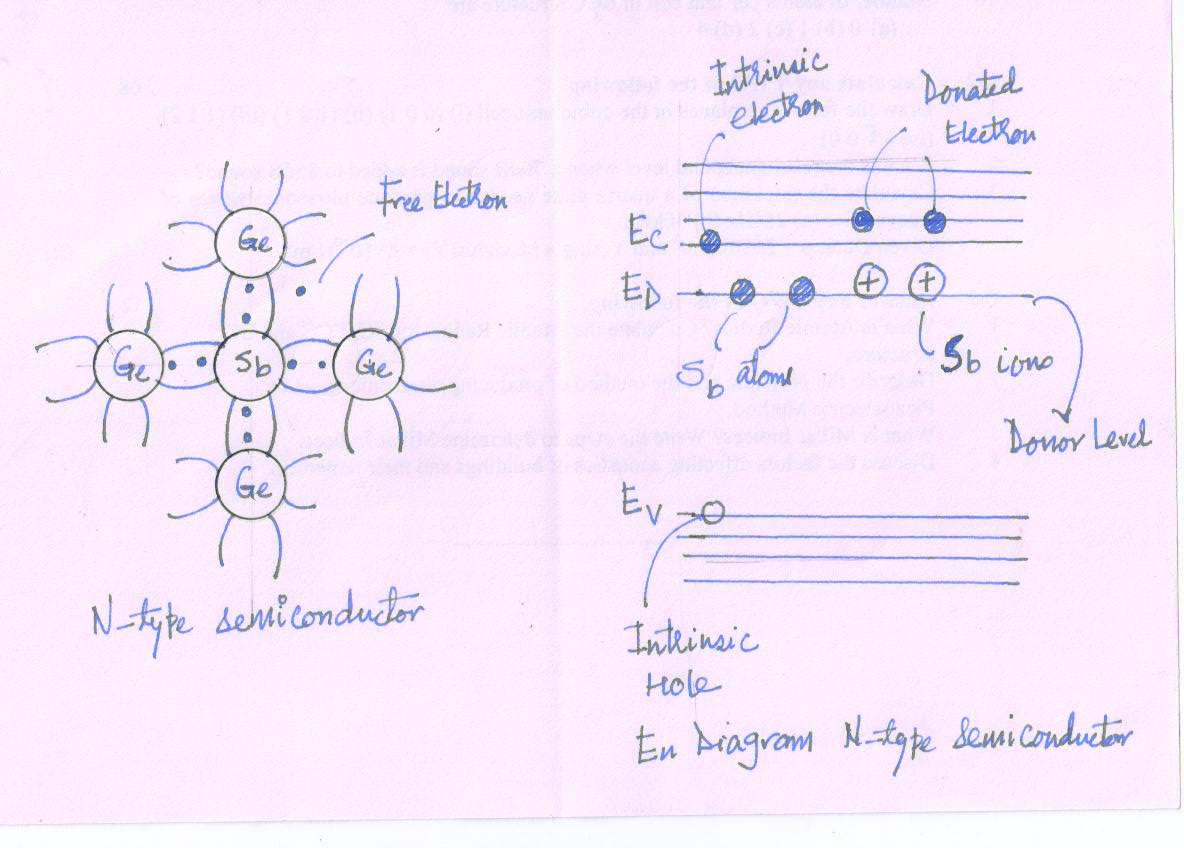
- Consider a crystal of Ge in which a small fraction of Ge atoms is replaced by Sb atoms. The Sb atom is pentavalent and it occupies normal Ge lattice site. It forms four covalent bonds with four neighboring Ge atoms. Fig.

-
The fifth electron, not used in bonding, is loosely bound. With supply of little energy, it can be made free leaving behind a positively charged immobile ion.
-
Thus the impurity atoms donate free electrons to the crystal thereby increasing the conductivity of material. Hence they are called the donor impurities.
-
The conductivity is due to the negatively charged electrons. Hence, the material is called N-Type semiconductor.
-
The electron and hole pairs are generated in Ge due to thermal energy.
-
For N-Type of semiconductor, the concentration of free electron is far greater than concentration of holes. The addition of donor impurity generates new energy levels in the band picture. The donor energy levels of neutral donor atoms lie very close to the lower edge of conduction band.
-
With the supply of a little energy the neutral donor atom loses the fifth electron for conduction and it gets positively charged.
P-Type of semiconductors
-
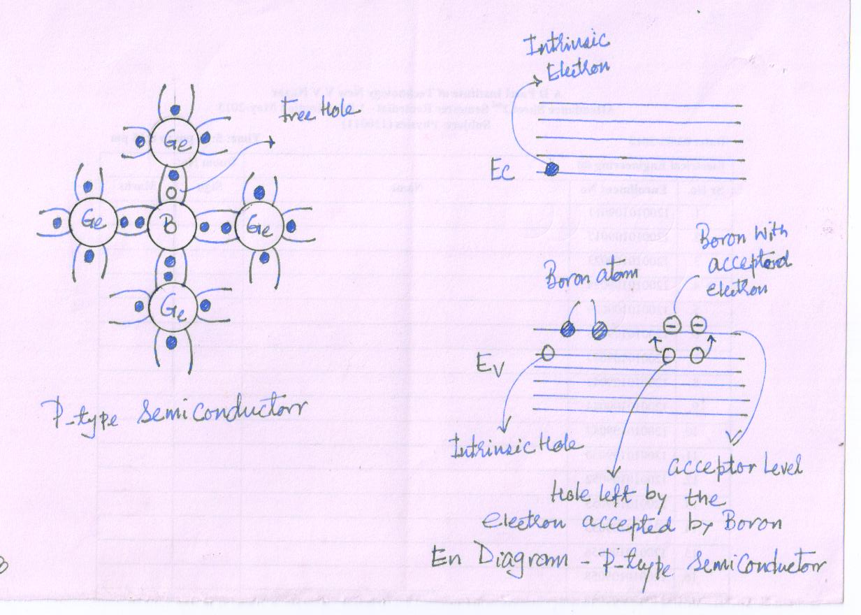
If the intrinsic semiconducting material, says Germanium, is doped by atoms of trivalent element like Boron, then the impurity atoms occupy places in the lattice which were previously occupied by Ge in pure crystal. Fig.10(4)

-
Boron, is being trivalent, is one electron short of being able to complete the stable structure. The absence of electron in one of these bond is hole. With a small amount of energy, it can accept an electron from the neighboring germanium atom and the vacancy shifts there.
-
The impurity atoms thus supply holes which are ready to accept electrons. Hence the impurity is known as acceptor impurity. The hole concentration is much more than electron concentration (thermally generated). The conductivity is due to the positively charged holes. Hence the semiconductor is called P-Type of semiconductor.
-
The addition of impurity introduces additional acceptor energy level, in the band diagram, slightly above the top of the conduction band.
-
With the supply of little energy, these vacancies can be occupied by electrons in valence band and thus increases the hole in valence band.
-
It should be remembered that even though the conduction in P-Type and N-Type materials is due to holes and electrons respectively. It does not mean that P-Type material has a positive charge and N-Type material has a negative charge.
-
The extrinsic semiconductors are electrically neutral at any given temperature.