Site pages
Current course
Participants
General
MODULE 1. Introduction to production of agricultur...
MODULE 2. Advance in material for tractor and agri...
MODULE 3. Advanced manufacturing techniques
MODULE 4. Heat treatment of steel
MODULE 5. Industrial lay out planning and quality ...
MODULE 6. Economics of process
MODULE 7. Techno economic feasibility of project r...
MODULE 8. Servo motors, drives and controllers
MODULE 9. CNC controllers for machine tools
MODULE 10. CNC programming
MODULE 11. Assembly and plant automation storage a...
LESSON 12 .CHEMICAL VAPOUR DEPOSITION (CVD)
4.1. Introduction
Chemical vapor deposition (CVD) is a chemical process used to produce high-purity, high-performance solid materials. The process is often used in the semiconductor industry to produce thin films. In a typical CVD process, the wafer (substrate) is exposed to one or more volatile precursors, which react and/or decompose on the substrate surface to produce the desired deposit. Frequently, volatile by-products are also produced, which are removed by gas flow through the reaction chamber.
Micro fabrication processes widely use CVD to deposit materials in various forms, including: monocrystalline, polycrystalline, amorphous, and epitaxial. These materials include: silicon, carbon fiber, carbon nano fibers, filaments, carbon nanotubes, SiO2, silicon-germanium, tungsten, silicon carbide, silicon nitride, silicon oxynitride, titanium nitride, and various high-k dielectrics. The CVD process is also used to produce synthetic diamonds.
Chemical vapour deposition or CVD is a generic name for a group of processes that involve depositing a solid material from a gaseous phase and is similar in some respects to physical vapour deposition (PVD). PVD differs in that the precursors are solid, with the material to be deposited being vaporised from a solid target and deposited onto the substrate.
Chemical gas sources are thermally, optically, or electrically (plasma) reacted with a surface to “leave” behind deposits with reaction byproducts pumped out of the reaction tube or vacuum chamber.
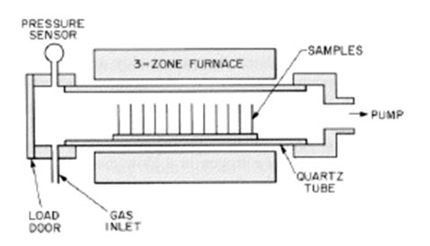
Fig. 4.4.1. Schematic diagram of CVD Hot wall- reduced pressure reactor
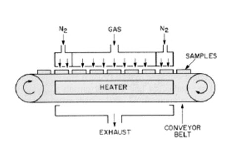
Fig. 4.4.2 schematic diagram of CVD Continous- atmospheric pressure reactor
4.2. Types of CVD Processes
CVD covers processes such as
Atmospheric Pressure Chemical Vapour Deposition (APCVD)
Low Pressure Chemical Vapour Deposition (LPCVD)
Metal-Organic Chemical Vapour Deposition (MOCVD)
Plasma Assisted Chemical Vapour Deposition (PACVD) or Plasma Enhanced Chemical Vapour Deposition (PECVD)
Laser Chemical Vapour Deposition (LCVD)
Photochemical Vapour Deposition (PCVD)
Chemical Vapour Infiltration (CVI)
Chemical Beam Epitaxy (CBE)
4.2.1. Atmospheric Pressure CVD (APCVD)
With the CVD method under atmospheric pressure (atmospheric pressure CVD; PCVD), without evacuation of the process plant, at a temperature of about 400 ° C oxide layers possibly together with foreign substances isolated. The required elements silicon and oxygen are the gases Silane SiH4 and O2 by adding nitrogen. To Siliziumoxid bildung then run the following reactions:
SiH4 + 2O2 -> SiO2 + 2H2O
SiH4 + O2> 2H2 + SiO2
Because of the low temperature process are only small values of conformity, so that edges with significantly less material to be covered than the horizontal surfaces. By the addition of ozone is the dynamics of particles anlagernden influenced so that their agility on the substrate. Dick differences can be balanced and thus compliance should be increased.
To defuse the following in the structuring of the oxide layer resulting sharp edges, achieved by the addition of gases phosphine and Diboran the integration of phosphorus and boron in the Oxidstruktur. This is below the melting point of 900 °C humiliated, so that by momentary melting of the hard layer breaks defused. This is for the quality of metal contacts that angry at highly miniaturized structures important.
Advantages : High deposition rates, simple, high throughput
Disadvantages : Poor uniformity, purity is less than LPCVD
Use : mainly for thick oxides.
4.2.2. Low Pressure CVD (LPCVD)
In this application for the production of films with low thickness of silicon, nitrides, but also of polysilicon and tungsten, the plant evacuated reaction (correspondingly low pressure CVD, LPCVD). Among the low-pressure conditions (in the range 10 to 100 Pa) is the movement dynamics considerably more favorable for the deposition of layers of conformity as high as under atmospheric pressure. Through mutual clashes are also Gaspartikel here by the linear movement discouraged. The average distance between collisions, however, lies in the range of centimeters, so that together with the high mobility of the deposited particles in the high process temperature of 900 °C is the material into low-lying areas can penetrate. Thus, a uniform deposition. There may be values of the conformity of a K near achieved (upto 0.98).
The procedure exceeds the APCVD technology reached regarding the density and electrical quality.
Advantages : Excellent uniformity, purity
Disadvantages : Lower (but reasonable) deposition rates than APCVD
Use : for polysilicon deposition, dielectric layer deposition, and doped dielectric deposition.
It can be used for a variety of materials:
Polysilicon for gate contacts
Thick oxides used for isolation between metal interconnects
Doped oxides useful for global planarization
Nitrides and other dielectrics for isolation or capacitors
Metals for seed layers for vias and interconnect lines
4.2.3. Metal Organic CVD (MOCVD)
Advantages : Highly flexible—> can deposit semiconductors, metals, dielectrics
Disadvantages : HIGHLY TOXIC!, Very expensive source material. Environmental disposal costs are high.
Uses : Dominates optical (but not electronic) III-V technology, some metalization processes (W plugs and Cu)
4.2.4. Plasma Enhanced CVD (PECVD)
With the plasma enhanced CVD process is the deposition at temperatures around 300°C allows, which does not destroy other structures (such as aluminum structures, which at 500°C melt). The temperature in this alone will not onset of decomposition reactions of the process gases will be through encouragement of a plasma with high frequency electric fields triggered.
The silicon is on the gas SiH2Cl2, of which it is at relatively low temperatures separates. With the support of the plasma excitation are the low process temperatures at 300 ° C is possible.
The deposition of SiO2 and silicon nitride Si3N4 at low conformity (k <0.8) but high growth speed (up to 500 nm / min), is hereby possible.
It can process multiple installations by a gripper automated control. These are the wafer into a warehouse. From there they will then lock on an interim, the pressure differences bridged in the process of the separation chamber passed. Plasmas are used to force reactions that would not be possible at low temperature.
Advantages : Uses low temperatures necessary for rear end processing.
Disadvantages : Plasma damage typically results.
Use : for dielectrics coatings.
4.3. Coating Characteristics
CVD coatings are typically:
Fine grained
Impervious
High purity
Harder than similar materials produced using conventional ceramic fabrication processes
CVD coatings are usually only a few microns thick and are generally deposited at fairly slow rates, usually of the order of a few hundred microns per hour.
4.4. CVD Apparatus
A CVD apparatus will consist of several basic components:
-
Gas delivery system: For the supply of precursors to the reactor chamber
-
Reactor chamber: Chamber within which deposition takes place
-
Substrate loading mechanism: A system for introducing and removing substrates, mandrels etc
-
Energy source: Provide the energy/heat that is required to get the precursors to react/decompose.
-
Vacuum system: A system for removal of all other gaseous species other than those required for the reaction/deposition.
-
Exhaust system: System for removal of volatile by-products from the reaction chamber.
-
Exhaust treatment systems: In some instances, exhaust gases may not be suitable for release into the atmosphere and may require treatment or conversion to safe/harmless compounds.
-
Process control equipment: Gauges, controls etc to monitor process parameters such as pressure, temperature and time. Alarms and safety devices would also be included in this category.
4.5. Energy Sources
There are several suitable sources of heat for CVD processes. These include:
-
Resistive Heating e.g. tube furnaces
-
Radiant Heating e.g. halogen lamps
-
Radio Frequency Heating e.g. induction heating
-
Lasers
-
Other energy sources may include UV-visible light or lasers as a source of photo energy.
4.6. Precursors
Precursor gases (often diluted in carrier gases) are delivered into the reaction chamber at approximately ambient temperatures. As they pass over or come into contact with a heated substrate, they react or decompose forming a solid phase which and are deposited onto the substrate. The substrate temperature is critical and can influence what reactions will take place.
Materials are deposited from the gaseous state during CVD. Thus precursors for CVD processes must be volatile, but at the same time stable enough to be able to be delivered to the reactor. Generally precursor compounds will only provide a single element to the deposited material, with others being volatilised during the CVD process. However sometimes precursors may provide more than one. Such materials simplify the delivery system, as they reduce the number of reactants required to produce a given compound.
Typical Precursor Materials
CVD precursor materials fall into a number of categories such as:
Halides - TiCl4, TaCl5, WF6, etc
Hydrides - SiH4, GeH4, AlH3(NMe3)2, NH3, etc
Metal Organic Compounds
Metal Alkyls - AlMe3, Ti(CH2tBu)4, etc
Metal Alkoxides - Ti(OiPr)4, etc
Metal Dialylamides - Ti(NMe2)4, etc
Metal Diketonates - Cu(acac)2, etc
Metal Carbonyls - Ni(CO)4, etc
Others – include a range of other metal organic compounds, complexes and ligands.
Materials That Can be Produced by CVD Processes
CVD is an extremely versatile process that can be used to process almost any metallic or ceramic compound. Some of these include:
Elements
Metals and alloys
Carbides
Nitrides
Borides
Oxides
Intermetallic compounds
CVD Gas Products
An often neglected by-product of the CVD process are volatile gases. However, these gases may be toxic, flammable or corrosive so must be treated appropriately. Analysis of the off-gases can also lead to a better understanding of the CVD reaction mechanisms and the information used to refine the process.
4.7. Applications
CVD has applications across a wide range of industries such as:
-
Coatings: Coatings for a variety of applications such as wear resistance, corrosion resistance, high temperature protection, erosion protection and combinations thereof.
-
Semiconductors and related devices: Integrated circuits, sensors and optoelectronic devices
-
Dense structural parts: CVD can be used to produce components that are difficult or uneconomical to produce using conventional fabrication techniques. Dense parts produced via CVD are generally thin walled and maybe deposited onto a mandrel or former.
-
Optical Fibers: For telecommunications.
-
Composites: Preforms can be infiltrated using CVD techniques to produce ceramic matrix composites such as carbon-carbon, carbon-silicon carbide and silicon carbide-silicon carbide composites. This process is sometimes called chemical vapour infiltration or CVI.
-
Powder production: Production of novel powders and fibres
-
Catalysts
-
Nanomachines
Last modified: Tuesday, 29 April 2014, 9:38 AM